Closed Dec 25th-26th
800-300-1968
We Stock Hard to Find Parts
My Account
|
My Orders
|
My Cart
Questions?
(800) 300-1968
Register
(current)
My Account
(current)
My Orders
(current)
My Cart
(current)
Categories
(current)
Manufacturers
Request a Quote
Sell Your Excess
Consignment
Quality Assurance
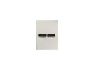
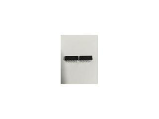
74ACTQ244M
Part #
74ACTQ244M
Description
Category
IC
Availability
In Stock
Qty
44
Qty
Price
1 - 9
$2.29478
10 - 18
$1.82539
19 - 27
$1.72109
28 - 36
$1.59939
37 +
$1.42555
Manufacturer
Available
Qty
National Semiconductor Corp
Freelance Stock:
44
Ships Immediately
Add to Cart
Related Items
National Semiconductor Corp
IC
74ACT00
$6.33069
National Semiconductor Corp
IC
74ACT004PC
National Semiconductor Corp
IC
74ACT00PC
$0.22684
National Semiconductor Corp
IC
74ACT00SC
$0.29604
National Semiconductor Corp
IC
74ACT00SC-ND
$1.06077
Fairchild Semiconductor
IC
74ACT02
$9.64328