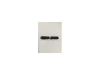
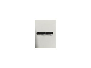
Freelance Electronics Components Distributor
Closed Dec 25th-26th
800-300-1968
We Stock Hard to Find Parts

74ACT16244DGGR

Part # 74ACT16244DGGR
Description IC, 16-BIT BUFFER/LINE DRIVERTSSOP-48
Category IC
Availability In Stock
Qty 1745
Qty Price
1 - 78 $1.91818
79 - 196 $1.52583
197 - 382 $1.43864
383 - 579 $1.33692
580 + $1.19160
Manufacturer Available Qty
Texas Instruments
Date Code: 9709
  • Shipping Freelance Stock: 1745
    Ships Immediately


Technical Document


DISCLAIMER: The information provided herein is solely for informational purposes. Customers must be aware of the suitability of this product for their application, and consider that variable factors such as Manufacturer, Product Category, Date Codes, Pictures and Descriptions may differ from available inventory.

SN54ACT16244, 74ACT16244
16-BIT BUFFERS/LINE DRIVERS
WITH 3-STATE OUTPUTS
SCAS116B – MARCH 1990 – REVISED APRIL 1996
1
POST OFFICE BOX 655303 DALLAS, TEXAS 75265
Members of the Texas Instruments
Widebus
Family
Inputs Are TTL-Voltage Compatible
3-State Outputs Drive Bus Lines or Buffer
Memory Address Registers
Flow-Through Architecture Optimizes
PCB Layout
Distributed V
CC
and GND Pin
Configurations Minimize High-Speed
Switching Noise
EPIC
(Enhanced-Performance Implanted
CMOS) 1- m Process
500-mA Typical Latch-Up Immunity at
125°C
Package Options Include Plastic Shrink
Small-Outline (DL) and Thin Shrink
Small-Outline (DGG) Packages, and 380-mil
Fine-Pitch Ceramic Flat (WD) Packages
Using 25-mil Center-to-Center Pin Spacings
description
The SN54ACT16244 and 74ACT16244 are 16-bit
buffers/line drivers designed specifically to
improve both the performance and density of
3-state memory address drivers, clock drivers,
and bus-oriented receivers and transmitters.
They can be used as four 4-bit buffers, two 8-bit
buffers, or one 16-bit buffer. The devices provide
true outputs and symmetrical OE
(active-low)
output-enable inputs.
The 74ACT16244 is packaged in TI’s shrink small-outline package, which provides twice the I/O pin count and
functionality of standard small-outline packages in the same printed-circuit-board area.
The SN54ACT16244 is characterized for operation over the full military temperature range of –55°C to 125°C.
The 74ACT16244 is characterized for operation from –40°C to 85°C.
FUNCTION TABLE
(each driver)
INPUTS
OUTPUT
OE
A
Y
L H H
L LL
H X Z
Copyright 1996, Texas Instruments Incorporated
PRODUCTION DATA information is current as of publication date.
Products conform to specifications per the terms of Texas Instruments
standard warranty. Production processing does not necessarily include
testing of all parameters.
Please be aware that an important notice concerning availability, standard warranty, and use in critical applications of
Texas Instruments semiconductor products and disclaimers thereto appears at the end of this data sheet.
EPIC and Widebus are trademarks of Texas Instruments Incorporated.
1
2
3
4
5
6
7
8
9
10
11
12
13
14
15
16
17
18
19
20
21
22
23
24
48
47
46
45
44
43
42
41
40
39
38
37
36
35
34
33
32
31
30
29
28
27
26
25
1OE
1Y1
1Y2
GND
1Y3
1Y4
V
CC
2Y1
2Y2
GND
2Y3
2Y4
3Y1
3Y2
GND
3Y3
3Y4
V
CC
4Y1
4Y2
GND
4Y3
4Y4
4OE
2OE
1A1
1A2
GND
1A3
1A4
V
CC
2A1
2A2
GND
2A3
2A4
3A1
3A2
GND
3A3
3A4
V
CC
4A1
4A2
GND
4A3
4A4
3OE
SN54ACT16244 . . . WD PACKAGE
74ACT16244 . . . DGG OR DL PACKAGE
(TOP VIEW)
SN54ACT16244, 74ACT16244
16-BIT BUFFERS/LINE DRIVERS
WITH 3-STATE OUTPUTS
SCAS116B – MARCH 1990 – REVISED APRIL 1996
2
POST OFFICE BOX 655303 DALLAS, TEXAS 75265
logic symbol
47
1A1
46
1A2
44
1A3
43
1A4
1Y1
2
1Y2
3
1Y3
5
1Y4
6
41
2A1
40
2A2
38
2A3
37
2A4
2Y1
8
2Y2
9
2Y3
11
2Y4
12
36
3A1
35
3A2
33
3A3
32
3A4
3Y1
13
3Y2
14
3Y3
16
3Y4
17
30
4A1
29
4A2
27
4A3
26
4A4
4Y1
19
4Y2
20
4Y3
22
4Y4
23
EN1
1
EN4
24
1
2
4
1
1
1
1
1OE
2OE
3OE
4OE
EN2
48
EN3
25
This symbol is in accordance with ANSI/IEEE Std 91-1984 and IEC Publication 617-12.
3
SN54ACT16244, 74ACT16244
16-BIT BUFFERS/LINE DRIVERS
WITH 3-STATE OUTPUTS
SCAS116B – MARCH 1990 – REVISED APRIL 1996
3
POST OFFICE BOX 655303 DALLAS, TEXAS 75265
logic diagram (positive logic)
1OE
1
1A1
1A2
1A3
1A4
47
46
44
43
1Y1
1Y2
1Y3
1Y4
2
3
5
6
2OE
48
2A1
2A2
2A3
2A4
41
40
38
37
2Y1
2Y2
2Y3
2Y4
8
9
11
12
3OE
25
3A1
3A2
3A3
3A4
36
35
33
32
3Y1
3Y2
3Y3
3Y4
13
14
16
17
4OE
24
4A1
4A2
4A3
4A4
30
29
27
26
4Y1
4Y2
4Y3
4Y4
19
20
22
23
absolute maximum ratings over operating free-air temperature range (unless otherwise noted)
Supply voltage range, V
CC
–0.5 V to 7 V. . . . . . . . . . . . . . . . . . . . . . . . . . . . . . . . . . . . . . . . . . . . . . . . . . . . . . . . . .
Input voltage range, V
I
(see Note 1) –0.5 V to V
CC
+ 0.5 V. . . . . . . . . . . . . . . . . . . . . . . . . . . . . . . . . . . . . . . . . . .
Output voltage range, V
O
(see Note 1) –0.5 V to V
CC
+ 0.5 V. . . . . . . . . . . . . . . . . . . . . . . . . . . . . . . . . . . . . . . .
Input clamp current, I
IK
(V
I
< 0 or V
I
> V
CC
) ±20 mA. . . . . . . . . . . . . . . . . . . . . . . . . . . . . . . . . . . . . . . . . . . . . . . .
Output clamp current, I
OK
(V
O
< 0 or V
O
> V
CC
) ±50 mA. . . . . . . . . . . . . . . . . . . . . . . . . . . . . . . . . . . . . . . . . . . .
Continuous output current, I
O
(V
O
= 0 to V
CC
) ±50 mA. . . . . . . . . . . . . . . . . . . . . . . . . . . . . . . . . . . . . . . . . . . . . .
Continuous current through V
CC
or GND ±400 mA. . . . . . . . . . . . . . . . . . . . . . . . . . . . . . . . . . . . . . . . . . . . . . . . . .
Maximum power dissipation at T
A
= 55°C (in still air) (see Note 2): DGG package 0.85 W. . . . . . . . . . . . . . . .
DL package 1.2 W. . . . . . . . . . . . . . . . . . .
Storage temperature range, T
stg
–65°C to 150°C. . . . . . . . . . . . . . . . . . . . . . . . . . . . . . . . . . . . . . . . . . . . . . . . . . .
Stresses beyond those listed under “absolute maximum ratings” may cause permanent damage to the device. These are stress ratings only, and
functional operation of the device at these or any other conditions beyond those indicated under “recommended operating conditions” is not
implied. Exposure to absolute-maximum-rated conditions for extended periods may affect device reliability.
NOTES: 1. The input and output voltage ratings may be exceeded if the input and output current ratings are observed.
2. The maximum package power dissipation is calculated using a junction temperature of 150 C and a board trace length of 750 mils.
12345NEXT