Closed Dec 25th-26th
800-300-1968
We Stock Hard to Find Parts
My Account
|
My Orders
|
My Cart
Questions?
(800) 300-1968
Register
(current)
My Account
(current)
My Orders
(current)
My Cart
(current)
Categories
(current)
Manufacturers
Request a Quote
Sell Your Excess
Consignment
Quality Assurance
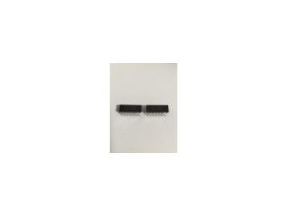
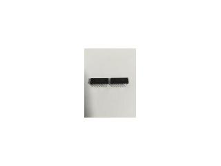
74ACT00P
Part #
74ACT00P
Description
Category
IC
Availability
Out of Stock
Qty
0
Related Items
National Semiconductor Corp
IC
74ACT00
$6.33069
National Semiconductor Corp
IC
74ACT004PC
National Semiconductor Corp
IC
74ACT00PC
$0.22684
National Semiconductor Corp
IC
74ACT00SC
$0.29604
National Semiconductor Corp
IC
74ACT00SC-ND
$1.06077
Fairchild Semiconductor
IC
74ACT02
$9.64328