Philips Semiconductors Product specification
74ABT16374B
74ABTH16374B
16-bit D-type flip-flop; positive-edge trigger
(3-State)
1998 Feb 27
4
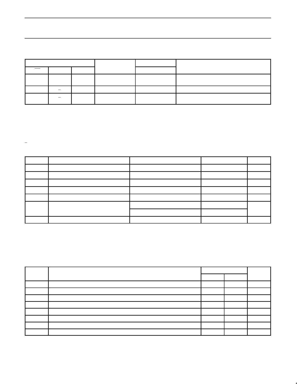
FUNCTION TABLE
INPUTS
INTERNAL
OUTPUTS
nOE nCP nDx
REGISTER
nQ0 – nQ7
L
L
↑
↑
l
h
L
H
L
H
Load and read register
L ↑ X NC NC Hold
H
H
↑
↑
X
nDx
NC
nDx
Z
Z
Disable outputs
H = High voltage level
h = High voltage level one set-up time prior to the High-to-Low E transition
L = Low voltage level
l = Low voltage level one set-up time prior to the High-to-Low E transition
NC= No change
X = Don’t care
Z = High impedance “off” state
↑ = Low-to-High clock transition
↑
= Not a Low-to-High clock transition
ABSOLUTE MAXIMUM RATINGS
1,
2
SYMBOL
PARAMETER CONDITIONS RATING UNIT
V
CC
DC supply voltage –0.5 to +7.0 V
I
IK
DC input diode current V
I
< 0 –18 mA
V
I
DC input voltage
3
–1.2 to +7.0 V
I
OK
DC output diode current V
O
< 0 –50 mA
V
OUT
DC output voltage
3
output in Off or High state –0.5 to +5.5 V
p
output in Low state 128
OUT
u
u
u
output in High state –64
T
stg
Storage temperature range –65 to 150 °C
NOTES:
1. Stresses beyond those listed may cause permanent damage to the device. These are stress ratings only and functional operation of the
device at these or any other conditions beyond those indicated under “recommended operating conditions” is not implied. Exposure to
absolute-maximum-rated conditions for extended periods may affect device reliability.
2. The performance capability of a high-performance integrated circuit in conjunction with its thermal environment can create junction
temperatures which are detrimental to reliability. The maximum junction temperature of this integrated circuit should not exceed 150°C.
3. The input and output voltage ratings may be exceeded if the input and output current ratings are observed.
RECOMMENDED OPERATING CONDITIONS
LIMITS
MIN MAX
V
CC
DC supply voltage 4.5 5.5 V
V
I
Input voltage 0 V
CC
V
V
IH
High-level input voltage 2.0 V
V
IL
Low-level Input voltage 0.8 V
I
OH
High-level output current –32 mA
I
OL
Low-level output current 64 mA
∆t/∆v Input transition rise or fall rate 0 10 ns/V
T
amb
Operating free-air temperature range –40 +85 °C


