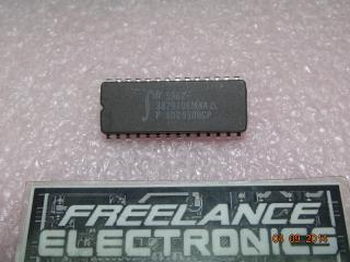
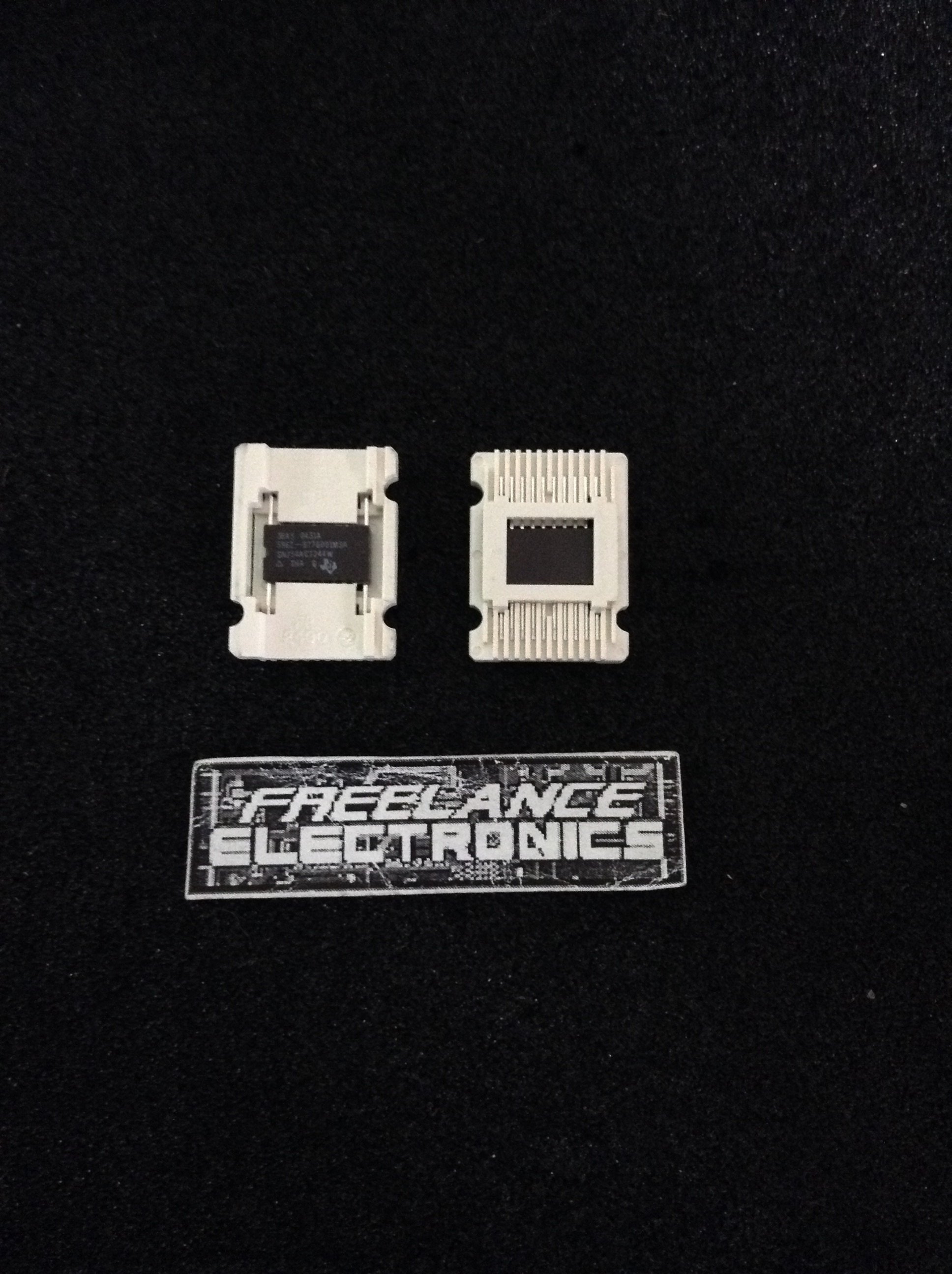
Freelance Electronics Components Distributor
Closed Dec 25th-26th
800-300-1968
We Stock Hard to Find Parts

5962-8776001MSA

Part # 5962-8776001MSA
Description Buffer/Line Driver 8-CH Non-Inverting 3-ST CMOS 20-Pin CFP
Category IC
Availability In Stock
Qty 20
Qty Price
1 - 4 $24.87969
5 - 8 $19.79066
9 - 12 $18.65977
13 - 16 $17.34039
17 + $15.45557
Manufacturer Available Qty
Texas Instruments
Date Code: 0431
  • Shipping Freelance Stock: 20
    Ships Immediately


Technical Document


DISCLAIMER: The information provided herein is solely for informational purposes. Customers must be aware of the suitability of this product for their application, and consider that variable factors such as Manufacturer, Product Category, Date Codes, Pictures and Descriptions may differ from available inventory.

SN54ACT244, SN74ACT244
OCTAL BUFFERS/DRIVERS
WITH 3-STATE OUTPUTS
SCAS517C – JUNE 1995 – REVISED OCTOBER 2002
1
POST OFFICE BOX 655303 DALLAS, TEXAS 75265
4.5-V to 5.5-V V
CC
Operation
Inputs Accept Voltages to 5.5 V
Max t
pd
of 9.5 ns at 5 V
Inputs Are TTL Compatible
SN54ACT244 ...J OR W PACKAGE
SN74ACT244 . . . DB, DW, N, NS, OR PW PACKAGE
(TOP VIEW)
3 2 1 20 19
9 10 11 12 13
4
5
6
7
8
18
17
16
15
14
1Y1
2A4
1Y2
2A3
1Y3
1A2
2Y3
1A3
2Y2
1A4
SN54ACT244 . . . FK PACKAGE
(TOP VIEW)
2Y4
1A1
1OE
1Y4
2A2 2OE
2Y1
GND
2A1
V
CC
1
2
3
4
5
6
7
8
9
10
20
19
18
17
16
15
14
13
12
11
1OE
1A1
2Y4
1A2
2Y3
1A3
2Y2
1A4
2Y1
GND
V
CC
2OE
1Y1
2A4
1Y2
2A3
1Y3
2A2
1Y4
2A1
description/ordering information
These octal buffers/drivers are designed specifically to improve the performance and density of 3-state memory
address drivers, clock drivers, and bus-oriented receivers and transmitters.
The ’ACT244 devices are organized as two 4-bit buffers/drivers with separate output-enable (OE
) inputs. When
OE
is low, the device passes noninverted data from the A inputs to the Y outputs. When OE is high, the outputs
are in the high-impedance state.
To ensure the high-impedance state during power up or power down, OE
should be tied to V
CC
through a pullup
resistor; the minimum value of the resistor is determined by the current-sinking capability of the driver.
ORDERING INFORMATION
T
A
PACKAGE
ORDERABLE
PART NUMBER
TOP-SIDE
MARKING
PDIP – N Tube SN74ACT244N SN74ACT244N
SOIC DW
Tube SN74ACT244DW
ACT244
40°Cto85°C
SOIC
DW
Tape and reel SN74ACT244DWR
ACT244
40°C
to
85°C
SOP – NS Tape and reel SN74ACT244NSR ACT244
SSOP – DB Tape and reel SN74ACT244DBR AD244
TSSOP – PW Tape and reel SN74ACT244PWR AD244
CDIP – J Tube SNJ54ACT244J SNJ54ACT244J
–55°C to 125°C
CFP – W Tube SNJ54ACT244W SNJ54ACT244W
LCCC – FK Tube SNJ54ACT24FK SNJ54ACT244FK
Package drawings, standard packing quantities, thermal data, symbolization, and PCB design guidelines are
available at www.ti.com/sc/package.
Copyright 2002, Texas Instruments Incorporated
PRODUCTION DATA information is current as of publication date.
Products conform to specifications per the terms of Texas Instruments
standard warranty. Production processing does not necessarily include
testing of all parameters.
Please be aware that an important notice concerning availability, standard warranty, and use in critical applications of
Texas Instruments semiconductor products and disclaimers thereto appears at the end of this data sheet.
On products compliant to MIL-PRF-38535, all parameters are tested
unless otherwise noted. On all other products, production
processing does not necessarily include testing of all parameters.
SN54ACT244, SN74ACT244
OCTAL BUFFERS/DRIVERS
WITH 3-STATE OUTPUTS
SCAS517C JUNE 1995 REVISED OCTOBER 2002
2
POST OFFICE BOX 655303 DALLAS, TEXAS 75265
FUNCTION TABLE
(each buffer)
INPUTS
OUTPUT
OE A
Y
L H H
L LL
H X Z
logic diagram (positive logic)
2OE
1
2
4
6
8
12
14
16
18
1A1
1A2
1A3
1A4
1Y1
1Y2
1Y3
1Y4
1OE
19
11
13
15
17
3
5
7
9
2A1
2A2
2A3
2A4
2Y1
2Y2
2Y3
2Y4
absolute maximum ratings over operating free-air temperature range (unless otherwise noted)
Supply voltage range, V
CC
0.5 V to 7 V. . . . . . . . . . . . . . . . . . . . . . . . . . . . . . . . . . . . . . . . . . . . . . . . . . . . . . . . . .
Input voltage range, V
I
(see Note 1) 0.5 V to V
CC
+ 0.5 V. . . . . . . . . . . . . . . . . . . . . . . . . . . . . . . . . . . . . . . . . . .
Output voltage range, V
O
(see Note 1) 0.5 V to V
CC
+ 0.5 V. . . . . . . . . . . . . . . . . . . . . . . . . . . . . . . . . . . . . . . .
Input clamp current, I
IK
(V
I
< 0 or V
I
> V
CC
) ±20 mA. . . . . . . . . . . . . . . . . . . . . . . . . . . . . . . . . . . . . . . . . . . . . . . .
Output clamp current, I
OK
(V
O
< 0 or V
O
> V
CC
) ±20 mA. . . . . . . . . . . . . . . . . . . . . . . . . . . . . . . . . . . . . . . . . . . .
Continuous output current, I
O
(V
O
= 0 to V
CC
) ±50 mA. . . . . . . . . . . . . . . . . . . . . . . . . . . . . . . . . . . . . . . . . . . . . .
Continuous current through V
CC
or GND ±200 mA. . . . . . . . . . . . . . . . . . . . . . . . . . . . . . . . . . . . . . . . . . . . . . . . . .
Package thermal impedance, θ
JA
(see Note 2): DB package 70°C/W. . . . . . . . . . . . . . . . . . . . . . . . . . . . . . . . .
DW package 58°C/W. . . . . . . . . . . . . . . . . . . . . . . . . . . . . . . . .
N package 69°C/W. . . . . . . . . . . . . . . . . . . . . . . . . . . . . . . . . . .
NS package 60°C/W. . . . . . . . . . . . . . . . . . . . . . . . . . . . . . . . .
PW package 83°C/W. . . . . . . . . . . . . . . . . . . . . . . . . . . . . . . . .
Storage temperature range, T
stg
65°C to 150°C. . . . . . . . . . . . . . . . . . . . . . . . . . . . . . . . . . . . . . . . . . . . . . . . . . .
Stresses beyond those listed under absolute maximum ratings may cause permanent damage to the device. These are stress ratings only, and
functional operation of the device at these or any other conditions beyond those indicated under recommended operating conditions is not
implied. Exposure to absolute-maximum-rated conditions for extended periods may affect device reliability.
NOTES: 1. The input and output voltage ratings may be exceeded if the input and output current ratings are observed.
2. The package thermal impedance is calculated in accordance with JESD 51-7.
SN54ACT244, SN74ACT244
OCTAL BUFFERS/DRIVERS
WITH 3-STATE OUTPUTS
SCAS517C JUNE 1995 REVISED OCTOBER 2002
3
POST OFFICE BOX 655303 DALLAS, TEXAS 75265
recommended operating conditions (see Note 3)
SN54ACT244 SN74ACT244
UNIT
MIN MAX MIN MAX
UNIT
V
CC
Supply voltage 4.5 5.5 4.5 5.5 V
V
IH
High-level input voltage 2 2 V
V
IL
Low-level input voltage 0.8 0.8 V
V
I
Input voltage 0 V
CC
0 V
CC
V
V
O
Output voltage 0 V
CC
0 V
CC
V
I
OH
High-level output current 24 24 mA
I
OL
Low-level output current 24 24 mA
t/v Input transition rise or fall rate 8 8 ns/V
T
A
Operating free-air temperature 55 125 40 85 °C
NOTE 3: All unused inputs of the device must be held at V
CC
or GND to ensure proper device operation. Refer to the TI application report,
Implications of Slow or Floating CMOS Inputs, literature number SCBA004.
electrical characteristics over recommended operating free-air temperature range (unless
otherwise noted)
PARAMETER
TEST CONDITIONS
V
CC
T
A
= 25°C SN54ACT244 SN74ACT244
UNIT
PARAMETER
TEST
CONDITIONS
V
CC
MIN TYP MAX MIN MAX MIN MAX
UNIT
I
OH
= 50 µA
4.5 V 4.4 4.49 4.4 4.4
I
OH
=
50
µ
A
5.5 V 5.4 5.49 5.4 5.4
V
OH
I 24 A
4.5 V 3.86 3.7 3.76
V
V
OH
I
OH
= 24 mA
5.5 V 4.86 4.7 4.76
V
I
OH
= 50 mA
5.5 V 3.85
I
OH
= 75 mA
5.5 V 3.85
I
OL
=50µA
4.5 V 0.001 0.1 0.1 0.1
I
OL
=
50
µ
A
5.5 V 0.001 0.1 0.1 0.1
V
OL
I
OL
=24mA
4.5 V 0.36 0.5 0.44
V
V
OL
I
OL
=
24
mA
5.5 V 0.36 0.5 0.44
V
I
OL
= 50 mA
5.5 V 1.65
I
OL
= 75 mA
5.5 V 1.65
I
OZ
V
O
= V
CC
or GND 5.5 V ±0.25 ±5 ±2.5 µA
I
I
V
I
= V
CC
or GND 5.5 V ±0.1 ±1 ±1 µA
I
CC
V
I
= V
CC
or GND, I
O
= 0 5.5 V 4 80 40 µA
I
CC
One input at 3.4 V,
Other inputs at GND or V
CC
5.5 V 0.6 1.6 1.5 mA
C
i
V
I
= V
CC
or GND 5 V 2.5 pF
C
o
V
I
= V
CC
or GND 5 V 8 pF
Not more than one output should be tested at a time, and the duration of the test should not exceed 2 ms.
This is the increase in supply current for each input that is at one of the specified TTL voltage levels, rather than 0 V or V
CC
.
123456NEXT