Closed Dec 25th-26th
800-300-1968
We Stock Hard to Find Parts
My Account
|
My Orders
|
My Cart
Questions?
(800) 300-1968
Register
(current)
My Account
(current)
My Orders
(current)
My Cart
(current)
Categories
(current)
Manufacturers
Request a Quote
Sell Your Excess
Consignment
Quality Assurance
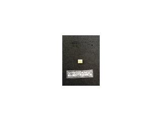
5962F9583402QXA
Part #
5962F9583402QXA
Description
Quad receiver: SMD. QML RadHardening
Category
IC
Availability
Out of Stock
Qty
0
Qty
Price
1 +
$350.00000
Related Items
National Semiconductor Corp
IC
5962F-8961501VHA
Aeroflex
IC
5962F-9583303VXA
$1092.11504
INTERSIL
IC
5962F0052301VYC
$551.49996
INTERSIL
IC
5962F0150901VPC
$1636.40679
INTERSIL
IC
5962F0150901VXC
$840.71523
INTERSIL
IC
5962F0151001VXC
$1968.94244