SLLS262N − JULY 1997 − REVISED MARCH 2004
1
POST OFFICE BOX 655303 • DALLAS, TEXAS 75265
D Meet or Exceed the Requirements of ANSI
TIA/EIA-644 Standard
D Operate With a Single 3.3-V Supply
D Designed for Signaling Rate of up to
400 Mbps
D Differential Input Thresholds ±100 mV Max
D Typical Propagation Delay Time of 2.1 ns
D Power Dissipation 60 mW Typical Per
Receiver at 200 MHz
D Bus-Terminal ESD Protection Exceeds 8 kV
D Low-Voltage TTL (LVTTL) Logic Output
Levels
D Pin Compatible With AM26LS32, MC3486,
and µA9637
D Open-Circuit Fail-Safe
description
The SN55LVDS32, SN65LVDS32,
SN65LVDS3486, and SN65LVDS9637 are
differential line receivers that implement the
electrical characteristics of low-voltage differential
signaling (LVDS). This signaling technique lowers
the output voltage levels of 5-V differential
standard levels (such as EIA/TIA-422B) to reduce
the power, increase the switching speeds, and
allow operation with a 3.3-V supply rail. Any of the
four differential receivers provides a valid logical
output state with a ±100-mV differential input
voltage within the input common-mode voltage
range. The input common-mode voltage range
allows 1 V of ground potential difference between
two LVDS nodes.
The intended application of these devices and
signaling technique is both point-to-point and
multidrop (one driver and multiple receivers) data
transmission over controlled impedance media of
approximately 100 Ω. The transmission media
may be printed-circuit board traces, backplanes,
or cables. The ultimate rate and distance of
data transfer depends on the attenuation
characteristics of the media and the noise
coupling to the environment.
The SN65LVDS32, SN65LVDS3486, and
SN65LVDS9637 are characterized for operation
from −40°C to 85°C. The SN55LVDS32 is
characterized for operation from −55°C to 125°C.
Copyright 1997 − 2004, Texas Instruments Incorporated
!"#$%! & '("")% $& ! *(+,'$%! -$%).
"!-('%& '!!"# %! &*)''$%!& *)" %/) %)"#& ! )0$& &%"(#)%&
&%$-$"- 1$""$%2. "!-('%! *"!')&&3 -!)& !% )')&&$",2 ',(-)
%)&%3 ! $,, *$"$#)%)"&.
Please be aware that an important notice concerning availability, standard warranty, and use in critical applications of
Texas Instruments semiconductor products and disclaimers thereto appears at the end of this data sheet.
1920132
17
18
16
15
14
1312119 10
5
4
6
7
8
4A
4Y
NC
G
3Y
1Y
G
NC
2Y
2A
1A
1B
NC
V
4B
GND
NC
3B
3A
2B
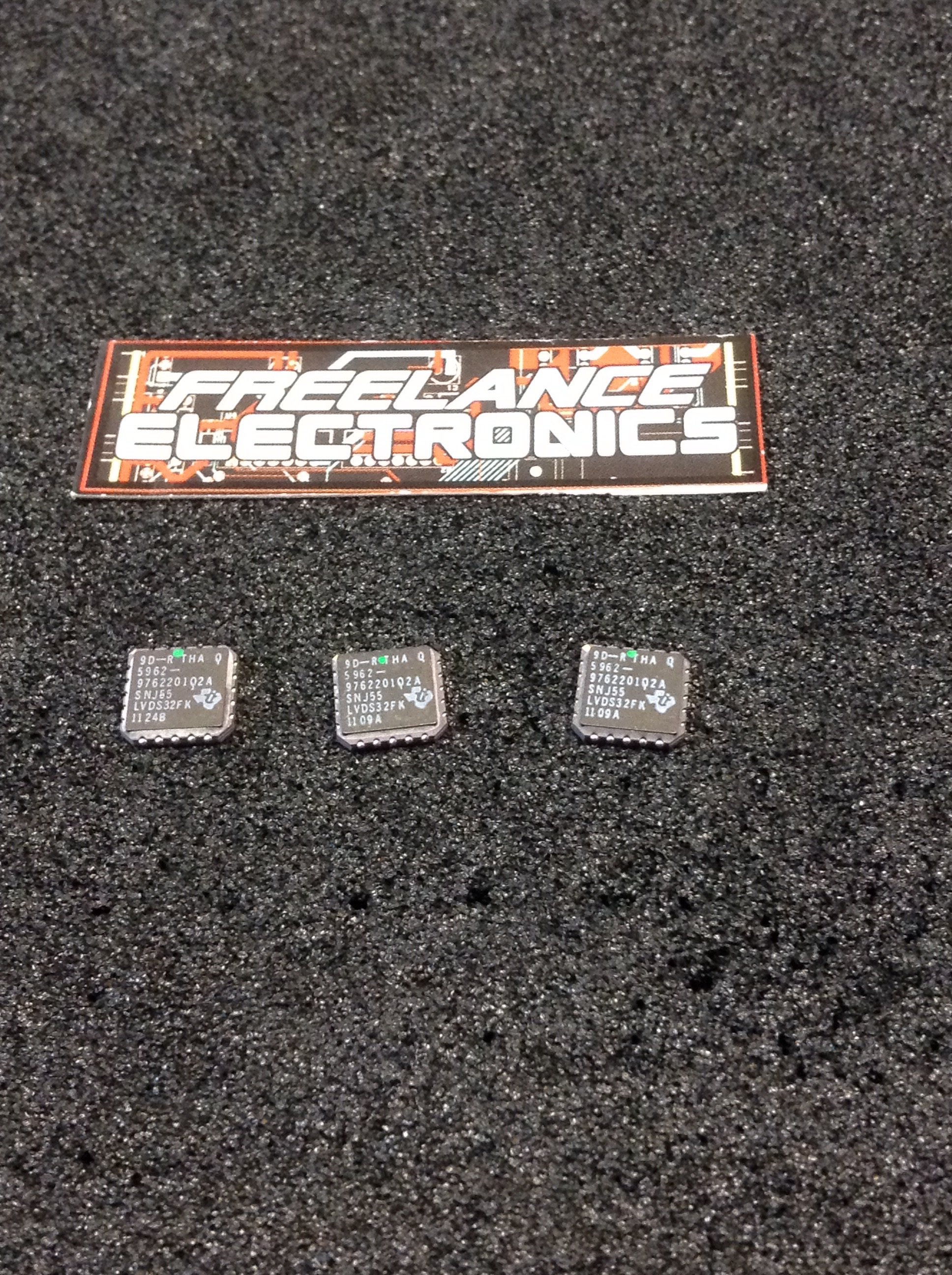
SN55LVDS32FK
(TOP VIEW)
CC
1
2
3
4
5
6
7
8
16
15
14
13
12
11
10
9
1B
1A
1Y
G
2Y
2A
2B
GND
V
CC
4B
4A
4Y
G
3Y
3A
3B
SN55LVDS32 ...J OR W
SN65LVDS32 ...D OR PW
(Marked as LVDS32 or 65LVDS32)
(TOP VIEW)
1
2
3
4
5
6
7
8
16
15
14
13
12
11
10
9
1B
1A
1Y
1,2EN
2Y
2A
2B
GND
V
CC
4B
4A
4Y
3,4EN
3Y
3A
3B
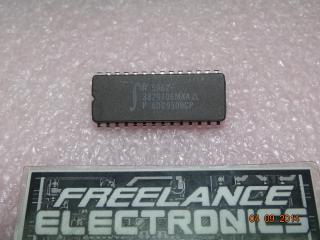
SN65LVDS3486D (Marked as LVDS3486)
(TOP VIEW)
1
2
3
4
8
7
6
5
V
CC
1Y
2Y
GND
1A
1B
2A
2B
SN65LVDS9637D (Marked as DK637 or LVDS37)
SN65LVDS9637DGN (Marked as L37)
SN65LVDS9637DGK (Marked as AXF)
(TOP VIEW)
*"!-('%& '!#*,$% %! 4 $,, *$"$#)%)"& $") %)&%)-
(,)&& !%/)"1&) !%)-. $,, !%/)" *"!-('%& *"!-('%!
*"!')&&3 -!)& !% )')&&$",2 ',(-) %)&%3 ! $,, *$"$#)%)"&.
PowerPAD is a trademark of Texas Instruments.