Closed Dec 25th-26th
800-300-1968
We Stock Hard to Find Parts
My Account
|
My Orders
|
My Cart
Questions?
(800) 300-1968
Register
(current)
My Account
(current)
My Orders
(current)
My Cart
(current)
Categories
(current)
Manufacturers
Request a Quote
Sell Your Excess
Consignment
Quality Assurance
AD10242BZ
Part #
AD10242BZ
Description
Category
HYBRID
Availability
Out of Stock
Qty
0
Qty
Price
1 +
$300.00000
Related Items
Analog Devices
IC
AD1021A
BAE SYSTEMS
HYBRID
101E1929G1
BAE SYSTEMS
HYBRID
101E1929G2
ANAREN / XINGER
HYBRID
1D1304-3
$11.43566
BOEING
HYBRID
280-26029-403
$974.07005
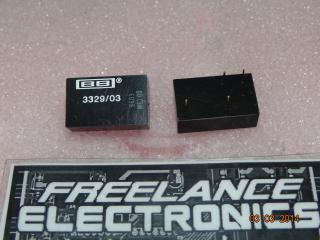
Burr-Brown Corporation
HYBRID
3329/03
$60.00000