Closed Dec 25th-26th
800-300-1968
We Stock Hard to Find Parts
My Account
|
My Orders
|
My Cart
Questions?
(800) 300-1968
Register
(current)
My Account
(current)
My Orders
(current)
My Cart
(current)
Categories
(current)
Manufacturers
Request a Quote
Sell Your Excess
Consignment
Quality Assurance
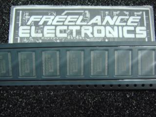
PCF8582C-2
Part #
PCF8582C-2
Description
Serial-I2C 2K-bit 8-Pin DIP256 x 8 3.3V/5V
Category
E-PROMS
Availability
Out of Stock
Qty
0
Qty
Price
1 +
$1.76320
Related Items
NXP SEMICONDUCTORS
IC
PCF8562TT/2
$4.85000
NXP SEMICONDUCTORS
IC
PCF8562TT/S400
$1.40263
NXP SEMICONDUCTORS
IC
PCF8562TT/S400/2
$5.50000
NXP SEMICONDUCTORS
IC
PCF8563T/F4
$1.08884
NXP SEMICONDUCTORS
IC
PCF8563T/F4,118
$0.58029
NXP SEMICONDUCTORS
IC
PCF8563TS/4
$0.66900