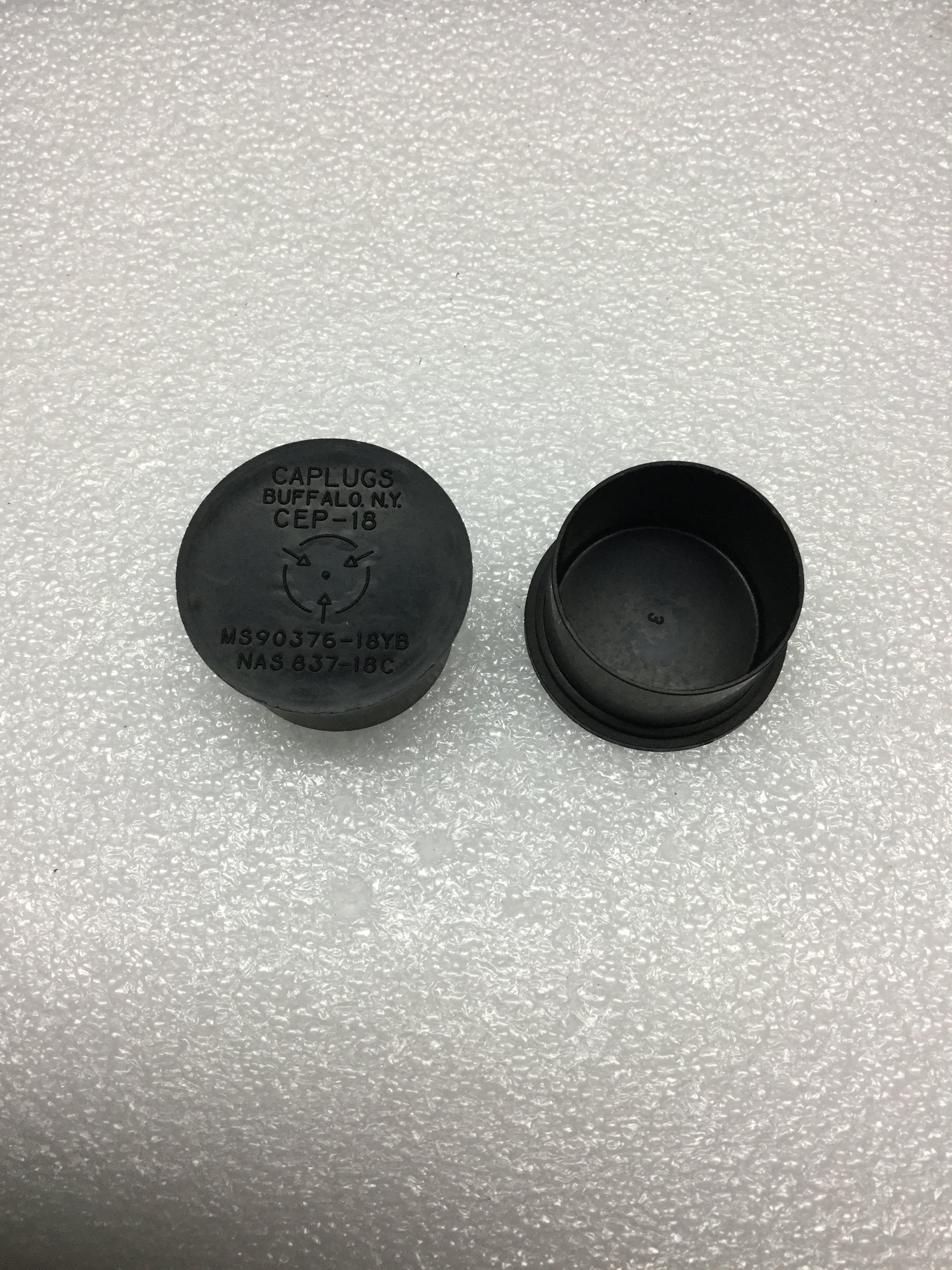
Freelance Electronics Components Distributor
Closed Dec 25th-26th
800-300-1968
We Stock Hard to Find Parts

CEP-18

Part # CEP-18
Description CAP, CONDUCTIVE , BLACKPLUG THREAD CONN 1-1/8-18
Category COVER
Availability In Stock
Qty 249
Qty Price
1 - 52 $0.21813
53 - 104 $0.17351
105 - 156 $0.16360
157 - 209 $0.15203
210 + $0.13551
Manufacturer Available Qty
Caplugs
  • Shipping Freelance Stock: 249
    Ships Immediately


Technical Document


DISCLAIMER: The information provided herein is solely for informational purposes. Customers must be aware of the suitability of this product for their application, and consider that variable factors such as Manufacturer, Product Category, Date Codes, Pictures and Descriptions may differ from available inventory.

CEP18N5/CEB18N5
CEF18N5
N-Channel Enhancement Mode Field Effect Transistor
FEATURES
Super high dense cell design for extremely low R
DS(ON)
.
High power and current handing capability.
ABSOLUTE MAXIMUM RATINGS T
c
= 25 C unless otherwise noted
Parameter Symbol
Limit
Units
Drain-Source Voltage
Gate-Source Voltage
Drain Current-Pulsed
a
Maximum Power Dissipation @ T
C
= 25 C
- Derate above 25 C
V
DS
V
GS
P
D
I
DM
e
500
1.8
219
72
11
±30
V
W
A
A
V
W/ C
1
S
G
D
G
S
D
CEB SERIES
TO-263(DD-PAK)
S
D
G
CEP SERIES
TO-220
CEF SERIES
TO-220F
S
D
G
Type V
DSS
R
DS(ON)
I
D
@V
GS
CEP18N5
CEF18N5
500V
500V
0.27Ω
0.27Ω
18A
18A
d
10V
10V
0.6
74
72
d
11
d
CEB18N5 500V 18A 10V
TO-220/263 TO-220F
PRELIMINARY
http://www.cetsemi.com
This is preliminary information on a new product in development now .
Details are subject to change without notice .
Rev 1. 2013.Jan.
0.27Ω
Drain Current-Continuous
I
D
A
@ T
C
= 100 C
@ T
C
= 25 C
18
18
d
Lead-free plating ; RoHS compliant.
Single Pulsed Avalanche Energy
e
Single Pulsed Avalanche Current
e
E
AS
I
AS
859
18
mJ
A
Operating and Store Temperature Range T
J
,T
stg
-55 to 150 C
Thermal Characteristics
Thermal Resistance, Junction-to-Case
Thermal Resistance, Junction-to-Ambient
Parameter Symbol Limit Units
C/W
C/W
62.5
0.57RθJC
RθJA
1.7
65
Electrical Characteristics T
c
= 25 C unless otherwise noted
Parameter Symbol Min Units
Off Characteristics
Drain-Source Breakdown Voltage
Zero Gate Voltage Drain Current
Gate Body Leakage Current, Forward
Gate Threshold Voltage
Static Drain-Source
On-Resistance
BV
DSS
I
DSS
IGSSR
I
GSSF
0.270.22
3 5
-100
100
1
V
nA
nA
µA
V
2
Gate Body Leakage Current, Reverse
On Characteristics
b
Dynamic Characteristics
c
Input Capacitance
Reverse Transfer Capacitance
Output Capacitance
Switching Characteristics
c
Turn-On Delay Time
Turn-Off Fall Time
Turn-Off Delay Time
Turn-On Rise Time
Total Gate Charge
Gate-Source Charge
Gate-Drain Charge
Drain-Source Diode Characteristics and Maximun Ratings
Drain-Source Diode Forward Current
Drain-Source Diode Forward Voltage
b
Test Condition
V
GS
= 0V, I
D
= 250µA
V
GS(th)
R
DS(on)
C
iss
C
oss
C
rss
t
d(on)
t
r
t
d(off)
t
f
Q
g
Q
gs
Q
gd
I
S
f
V
SD
g
Typ Max
500
V
DS
=500V, V
GS
= 0V
V
GS
= 30V, V
DS
= 0V
V
GS
= -30V, V
DS
= 0V
V
GS
= V
DS
, I
D
= 250µA
V
GS
= 10V, I
D
= 9A
V
DD
= 250V, I
D
=18A,
V
GS
= 10V, R
GEN
= 25
V
DS
= 400V,I
D
= 18A,
V
GS
= 10V
V
DS
= 25V, V
GS
= 0V,
f = 1.0 MHz
V
GS
= 0V, I
S
= 18A
3035
305
5
56
28
110
20
51
19
13
18
1.4
pF
pF
pF
ns
ns
ns
ns
nC
nC
nC
A
V
CEP18N5/CEB18N5
CEF18N5
e.L = 5.3mH, I
AS
=18A, V
DD
= 50V, R
G
= 25, Starting T
J
= 25 C
Notes :
a.Repetitive Rating : Pulse width limited by maximum junction temperature .
b.Pulse Test : Pulse Width < 300µs, Duty Cycle < 2% .
c.Guaranteed by design, not subject to production testing.
d.Limited only by maximum temperature allowed .
e.Pulse width limited by safe operating area .
f.Full package I
S(max)
=10A .
g.Full package V
SD
test condition I
S
=10A .
3
C, Capacitance (pF)
ID, Drain Current (A)
RDS(ON), Normalized
RDS(ON), On-Resistance(Ohms)
VDS, Drain-to-Source Voltage (V)
Figure 1. Output Characteristics
VGS, Gate-to-Source Voltage (V)
Figure 2. Transfer Characteristics
VDS, Drain-to-Source Voltage (V)
Figure 3. Capacitance
TJ, Junction Temperature( C)
Figure 4. On-Resistance Variation
with Temperature
2.6
2.2
1.8
1.4
1.0
0.6
0.2
V
GS
=10V
I
D
=9A
-100 -50 0 50 100 150 200
VTH, Normalized
Gate-Source Threshold Voltage
TJ, Junction Temperature( C)
Figure 5. Gate Threshold Variation
with Temperature
IS, Source-drain current (A)
VSD, Body Diode Forward Voltage (V)
Figure 6. Body Diode Forward Voltage
Variation with Source Current
C
rss
3900
3250
2600
1950
1300
650
0
0 5 10 15 20 25
C
iss
C
oss
24
16
8
0
0 2 4 6
32
8 10
T
J
=125 C
-55 C
25 C
20
16
12
8
4
0
0 5 10 2015
24
25 30
V
GS
=6V
V
GS
=5V
V
GS
=10,9,8,7V
0.4 0.6 0.8 1.0
10
0
10
-1
10
1
1.2 1.61.4
V
GS
=0
V
CEP18N5/CEB18N5
CEF18N5
1.3
1.2
1.1
1.0
0.9
0.8
0.7
0.6
V
DS
=V
GS
I
D
=250µA
-50 -25 0 25 50 75 100 125 150
175
12NEXT