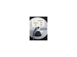
Freelance Electronics Components Distributor
Closed Dec 25th-26th
800-300-1968
We Stock Hard to Find Parts

IRF6644TRPBF

Part # IRF6644TRPBF
Description MOSFET, 100V, 60A, 13 MOHM, 35 NC QG, MED CAN - Tape and R
Category CONVERTER
Availability In Stock
Qty 902
Qty Price
1 - 189 $1.01835
190 - 378 $0.81005
379 - 568 $0.76377
569 - 757 $0.70976
758 + $0.63261
Manufacturer Available Qty
International Rectifier
Date Code: 1145
  • Shipping Freelance Stock: 902
    Ships Immediately


Technical Document


DISCLAIMER: The information provided herein is solely for informational purposes. Customers must be aware of the suitability of this product for their application, and consider that variable factors such as Manufacturer, Product Category, Date Codes, Pictures and Descriptions may differ from available inventory.

www.irf.com 1
8/18/06
DirectFET Power MOSFET
DirectFET ISOMETRIC
MN
Applicable DirectFET Outline and Substrate Outline (see p.7,8 for details)
Fig 1. Typical On-Resistance Vs. Gate Voltage
Typical values (unless otherwise specified)
Fig 2. Typical On-Resistance Vs. Drain Current
Description
The IRF6644PbF combines the latest HEXFET® Power MOSFET Silicon technology with the advanced DirectFET
TM
packaging to achieve the
lowest on-state resistance in a package that has the footprint of an SO-8 and only 0.7 mm profile. The DirectFET package is compatible with
existing layout geometries used in power applications, PCB assembly equipment and vapor phase, infra-red or convection soldering techniques,
when application note AN-1035 is followed regarding the manufacturing methods and processes. The DirectFET package allows dual sided
cooling to maximize thermal transfer in power systems, improving previous best thermal resistance by 80%.
The IRF6644PbF is optimized for primary side bridge topologies in isolated DC-DC applications, for wide range universal input Telecom
applications (36V - 75V), and for secondary side synchronous rectification in regulated DC-DC topologies. The reduced total losses in the device
coupled with the high level of thermal performance enables high efficiency and low temperatures, which are key for system reliability
improvements, and makes this device ideal for high performance isolated DC-DC converters.
Absolute Maximum Ratin
g
s
Parameter Units
V
DS
Drain-to-Source Voltage V
V
GS
Gate-to-Source Voltage
I
D
@ T
A
= 25°C
Continuous Drain Current, V
GS
@ 10V
I
D
@ T
A
= 70°C
Continuous Drain Current, V
GS
@ 10V
A
I
D
@ T
C
= 25°C
Continuous Drain Current, V
GS
@ 10V
I
DM
Pulsed Drain Current
E
AS
Single Pulse Avalanche Energy mJ
I
AR
Avalanche Current A
220
Max.
8.3
60
82
±20
100
10.3
6.2
4 6 8 10 12 14 16
V
GS
, Gate-to-Source Voltage (V)
0.00
0.02
0.04
0.06
0.08
T
y
p
i
c
a
l
R
D
S
(
o
n
)
,
(
)
T
J
= 25°C
T
J
= 125°C
I
D
= 6.2A
0 4 8 12 16 20
I
D
, Drain Current (A)
9
10
11
12
13
T
y
p
i
c
a
l
R
D
S
(
o
n
)
(
m
)
T
A
= 25°C
V
GS
= 8.0V
V
GS
= 7.0V
V
GS
= 10V
V
GS
= 15V
SH SJ SP MZ MN
V
DSS
V
GS
R
DS(on)
100V max ±20V max
10.3m@ 10V
Q
g tot
Q
gd
V
gs(th)
35nC 11.5nC 3.7V
PD - 97094A
IRF6644PbF
IRF6644TRPbF
l RoHS Compliant
l Lead-Free (Qualified up to 260°C Reflow)
l Application Specific MOSFETs
l Ideal for High Performance Isolated Converter
Primary Switch Socket
l Optimized for Synchronous Rectification
l Low Conduction Losses
l High Cdv/dt Immunity
l Low Profile (<0.7mm)
l Dual Sided Cooling Compatible
l Compatible with existing Surface Mount Techniques
Click on this section to link to the appropriate technical paper.
Click on this section to link to the DirectFET Website.
Surface mounted on 1 in. square Cu board, steady state.
T
C
measured with thermocouple mounted to top (Drain) of part.
Repetitive rating; pulse width limited by max. junction temperature.
Starting T
J
= 25°C, L = 12mH, R
G
= 25, I
AS
= 6.2A.
Notes:
IRF6644PbF
2 www.irf.com
Notes:
Repetitive rating; pulse width limited by max. junction temperature.
Pulse width 400µs; duty cycle 2%.
Static @ T
J
= 25°C (unless otherwise specified)
Parameter Min. Typ. Max. Units
BV
DSS
Drain-to-Source Breakdown Voltage 100 ––– ––– V
∆ΒV
DSS
/T
J
Breakdown Voltage Temp. Coefficient ––– 0.11 ––– V/°C
R
DS(on)
Static Drain-to-Source On-Resistance ––– 10.3 13
m
V
GS(th)
Gate Threshold Voltage 2.8 ––– 4.8 V
V
GS(th)
/T
J
Gate Threshold Voltage Coefficient ––– -10 ––– mV/°C
I
DSS
Drain-to-Source Leakage Current ––– ––– 20 µA
––– ––– 250
I
GSS
Gate-to-Source Forward Leakage ––– ––– 100 nA
Gate-to-Source Reverse Leakage ––– ––– -100
gfs Forward Transconductance 15 ––– ––– S
Q
g
Total Gate Charge ––– 35 47
Q
gs1
Pre-Vth Gate-to-Source Charge ––– 8.0 –––
Q
gs2
Post-Vth Gate-to-Source Charge ––– 1.6 ––– nC
Q
gd
Gate-to-Drain Charge ––– 11.5 17.3
Q
godr
Gate Charge Overdrive ––– 13 ––– See Fig. 15
Q
sw
Switch Charge (Q
gs2
+ Q
gd
)
––– 13.1 –––
Q
oss
Output Charge ––– 17 ––– nC
R
G
Gate Resistance
–––
1.0 2.0
t
d(on)
Turn-On Delay Time ––– 17 –––
t
r
Rise Time ––– 26 –––
t
d(off)
Turn-Off Delay Time ––– 34 ––– ns
t
f
Fall Time ––– 16 –––
C
iss
Input Capacitance ––– 2210 –––
C
oss
Output Capacitance ––– 420 ––– pF
C
rss
Reverse Transfer Capacitance ––– 100 –––
C
oss
Output Capacitance ––– 2120 –––
C
oss
Output Capacitance ––– 240 –––
Diode Characteristics
Parameter Min. Typ. Max. Units
I
S
Continuous Source Current ––– ––– 10
(Body Diode) A
I
SM
Pulsed Source Current ––– ––– 82
(Body Diode)d
V
SD
Diode Forward Voltage ––– ––– 1.3 V
t
rr
Reverse Recovery Time ––– 42 63 ns
Q
rr
Reverse Recovery Charge ––– 69 100 nC
MOSFET symbol
R
G
=6.2
V
DS
= 25V
Conditions
V
GS
= 0V, V
DS
= 80V, f=1.0MHz
V
GS
= 0V, V
DS
= 1.0V, f=1.0MHz
V
DS
= 16V, V
GS
= 0V
V
DD
= 50V, V
GS
= 10Vc
V
GS
= 0V
ƒ = 1.0MHz
I
D
= 6.2A
V
DS
= V
GS
, I
D
= 150µA
V
DS
= 100V, V
GS
= 0V
Conditions
V
GS
= 0V, I
D
= 250µA
Reference to 25°C, I
D
= 1mA
V
GS
= 10V, I
D
= 10.3A c
T
J
= 25°C, I
F
= 6.2A, V
DD
= 50V
di/dt = 100A/µs c
T
J
= 25°C, I
S
= 6.2A, V
GS
= 0V c
showing the
integral reverse
p-n junction diode.
I
D
= 6.2A
V
DS
= 80V, V
GS
= 0V, T
J
= 125°C
V
GS
= 20V
V
GS
= -20V
V
GS
= 10V
V
DS
= 10V, I
D
= 6.2A
V
DS
= 50V
IRF6644PbF
www.irf.com 3
Fig 3. Maximum Effective Transient Thermal Impedance, Junction-to-Ambient
1E-006 1E-005 0.0001 0.001 0.01 0.1 1 10 100
t
1
, Rectangular Pulse Duration (sec)
0.0001
0.001
0.01
0.1
1
10
100
T
h
e
r
m
a
l
R
e
s
p
o
n
s
e
(
Z
t
h
J
A
)
0.20
0.10
D = 0.50
0.02
0.01
0.05
SINGLE PULSE
( THERMAL RESPONSE )
Notes:
1. Duty Factor D = t1/t2
2. Peak Tj = P dm x Zthja + Tc
τ
J
τ
J
τ
1
τ
1
τ
2
τ
2
τ
3
τ
3
R
1
R
1
R
2
R
2
R
3
R
3
Ci i/Ri
Ci= τi/Ri
τ
τ
C
τ
4
τ
4
R
4
R
4
Ri (°C/W) τi (sec)
0.6784 0.00086
17.299 0.57756
17.566 8.94
9.4701 106
Absolute Maximum Ratin
g
s
Parameter Units
P
D
@T
A
= 25°C
Power Dissipation
W
P
D
@T
A
= 70°C
Power Dissipation
P
D
@T
C
= 25°C
Power Dissipation
T
P
Peak Soldering Temperature °C
T
J
Operating Junction and
T
STG
Storage Temperature Range
Thermal Resistance
Parameter Typ. Max. Units
R
θJA
Junction-to-Ambient ––– 45
R
θJA
Junction-to-Ambient 12.5 –––
R
θJA
Junction-to-Ambient 20 ––– °C/W
R
θJC
Junction-to-Case ––– 1.4
R
θJ-PCB
Junction-to-PCB Mounted 1.0 –––
270
-40 to + 150
Max.
89
2.8
1.8
Surface mounted on 1 in. square Cu board, steady state.
T
C
measured with thermocouple incontact with top (Drain) of part.
Used double sided cooling, mounting pad with large heatsink.
Notes:
Mounted on minimum footprint full size board with metalized
back and with small clip heatsink.
R
θ
is measured at T
J
of approximately 90°C.
Surface mounted on 1 in. square Cu
board (still air).
Mounted to a PCB with
small clip heatsink (still air)
Mounted on minimum
footprint full size board with
metalized back and with small
clip heatsink (still air)
1234NEXT