Closed Dec 25th-26th
800-300-1968
We Stock Hard to Find Parts
My Account
|
My Orders
|
My Cart
Questions?
(800) 300-1968
Register
(current)
My Account
(current)
My Orders
(current)
My Cart
(current)
Categories
(current)
Manufacturers
Request a Quote
Sell Your Excess
Consignment
Quality Assurance
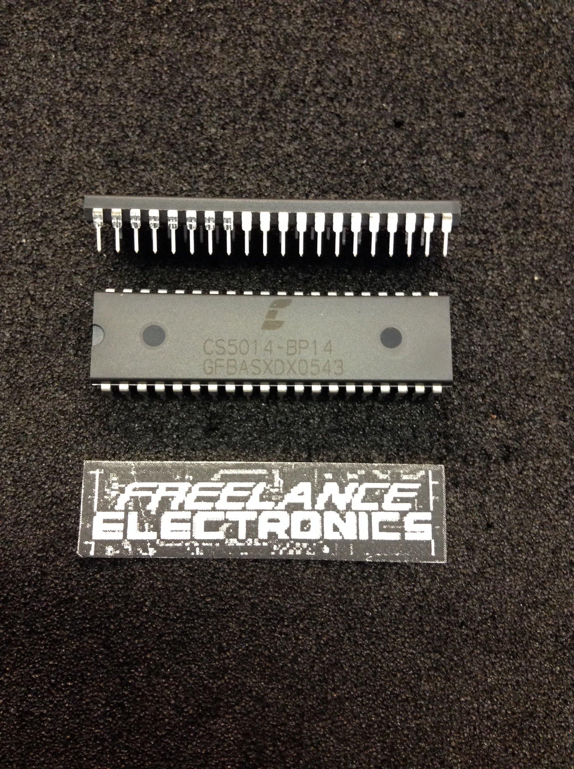
CS5014-BP14
Part #
CS5014-BP14
Description
A/D Converter 16, 14 & 12-BitSelf-Calibrating, 40pin PDip
Category
CONVERTER
Availability
Out of Stock
Qty
0
Qty
Price
1 +
$47.15156
Related Items
CRYSTAL
IC
CS5012A-BL12
$40.83788
CIRRUS TECHNIK GMBH
IC
CS5012A-KP7
$14.13619
PASCA II
CONVERTER
1-09364
RANTEC
CONVERTER
1002760-202
RANTEC
CONVERTER
1002760-205
FSCM
CONVERTER
1085AS762-1
$1,089.74087