Freelance Electronics Components Distributor
Closed Dec 25th-26th
800-300-1968
We Stock Hard to Find Parts

CS5014-BP14

Part # CS5014-BP14
Description A/D Converter 16, 14 & 12-BitSelf-Calibrating, 40pin PDip
Category CONVERTER
Availability Out of Stock
Qty 0
Qty Price
1 + $47.15156


Technical Document


DISCLAIMER: The information provided herein is solely for informational purposes. Customers must be aware of the suitability of this product for their application, and consider that variable factors such as Manufacturer, Product Category, Date Codes, Pictures and Descriptions may differ from available inventory.

Features
Monolithic CMOS A/D Converters
Microprocessor Compatible
Parallel and Serial Output
Inherent Track/Hold Input
True 12, 14 and 16-Bit Precision
Conversion Times:
CS5016 16.25
µ
s
CS5014 14.25
µ
s
CS5012A 7.20
µ
s
Self Calibration Maintains Accuracy
Over Time and Temperature
Low Power Dissipation: 150 mW
Low Distortion
General Description
The CS5012A/14/16 are 12, 14 and 16-bit monolithic
analog to digital converters with conversion times of
7.2
µ
s, 14.25
µ
s and 16.25
µ
s. Unique self-calibration cir-
cuitry insures excellent linearity and differential non-
linearity, with no missing codes. Offset and full scale
errors are kept within 1/2 LSB (CS5012A/14) and
1 LSB (CS5016), eliminating the need for calibration.
Unipolar and bipolar input ranges are digitally select-
able.
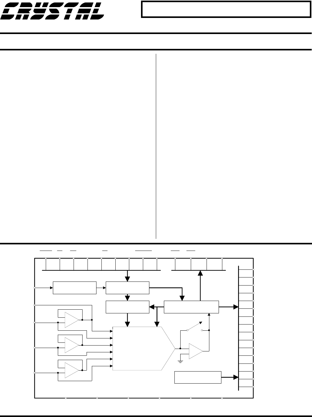
The pin compatible CS5012A/14/16 consist of a DAC,
conversion and calibration microcontroller, oscillator,
comparator, microprocessor compatible 3-state I/O,
and calibration circuitry. The input track-and-hold, in-
herent to the devices’ sampling architecture, acquires
the input signal after each conversion using a fast
slewing on-chip buffer amplifier. This allows throughput
rates up to 100 kHz (CS5012A), 56 kHz (CS5014) and
50 kHz (CS5016).
An evaluation board (CDB5012/14/16) is available
which allows fast evaluation of ADC performance.
ORDERING INFORMATION:
Pages 2-45, 2-46, & 2-47
MAR ’95
DS14F6
2-7
Crystal Semiconductor Corporation
P.O. Box 17847, Austin, TX 78760
(512) 445 7222 FAX: (512) 445 7581
16, 14 & 12-Bit, Self-Calibrating A/D Converters
Semiconductor Corporation
CS5016 CS5014 CS5012A
D5
D6
D7
D8
D9
D10
D11
D12
D13
D14
D15 (MSB)
D4 (LSB) CS5012A
6
7
8
9
12
13
14
15
16
17
18
19
D2 (LSB) CS5014
D0 (LSB) CS5016
D1
SCLKEOT EOC SDATA
2
3
4
5
37 38 39 40
D3
CLKIN
CLOCK
GENERATOR
20
INTRLV
34
RST
3221
A0
23
RD
22
HOLD
1
BW
3324
CAL
35
CS
BP/UP
REFBUF
AGND
29
VREF
28
AIN
26
27
CHARGE
REDISTRIBUTION
DAC
COMPARATOR
VA+ VA- VD+ VD- DGND TST
25 30 11 36 10 31
+
-
+
-
+
-
+
-
CONTROL
CALIBRATION
MEMORY
MICROCONTROLLER
STATUS REGISTER
Copyright
Crystal Semiconductor Corporation 1995
(All Rights Reserved)
CS5012A
CS5012A ANALOG CHARACTERISTICS (T
A
= T
MIN
to T
MAX
; VA+, VD+ = 5V;
VA-, VD- = -5V; VREF = 2.5V to 4.5V; f
clk
= 6.4 MHz for -7, 4 MHz for -12; Analog Source Impedance = 200)
CS5012A-K CS5012A-B CS5012-T
Parameter* Min Typ Max Min Typ Max Min Typ Max Units
Specified Temperature Range 0 to +70 -40 to +85 -55 to +125 °C
Accuracy
Linearity Error (Note 1)
Drift (Note 2)
±1/4
±1/8
±1/2 ±1/4
±1/8
±1/2 ±1/4
±1/8
±1/2
LSB
12
LSB
12
Differential Linearity (Note 1)
Drift (Note 2)
±1/4
±1/32
±1/2 ±1/4
±1/32
±1/2 ±1/4
±1/32
±1/2
LSB
12
LSB
12
Full Scale Error (Note 1)
Drift (Note 2)
±1/4
±1/16
±1/2 ±1/4
±1/16
±1/2 ±1/4
±1/8
±1/2
LSB
12
LSB
12
Unipolar Offset (Note 1)
Drift (Note 2)
±1/4
±1/16
±1/2 ±1/4
±1/16
±1/2 ±1/4
±1/16
±1/2
LSB
12
LSB
12
Bipolar Offset (Note 1)
Drift (Note 2)
±1/4
±1/16
±1/2 ±1/4
±1/16
±1/2 ±1/4
±1/16
±1/2
LSB
12
LSB
12
Bipolar Negative Full-Scale Error(Note 1)
Drift (Note 2)
±1/4
±1/16
±1/2 ±1/4
±1/16
±1/2 ±1/4
±1/16
±1/2
LSB
12
LSB
12
Total Unadjusted Error (Note 1)
Drift (Note 2)
±1/4
±1/4
±1/4
±1/4
±1/4
±1/4
LSB
12
LSB
12
Dynamic Performance (Bipolar Mode)
Peak Harmonic or (Note 1)
Spurious Noise
Full Scale, 1 kHz Input
Full Scale, 12 kHz Input
84
84
92
88
84
84
92
88
84
84
92
88
dB
dB
Total Harmonic Distortion 0.008 0.008 0.008 %
Signal-to-Noise Ratio (Note 1)
1 kHz, 0 dB Input
1 kHz, -60 dB Input
72 73
13
72 73
13
72 73
13
dB
dB
Noise (Note 3)
Unipolar Mode
Bipolar Mode
45
90
45
90
45
90
µV
rms
µV
rms
Notes: 1. Applies after calibration at any temperature within the specified temperature range.
2. Total drift over specified temperature range since calibration at power-up at 25 °C
3. Wideband noise aliased into the baseband. Referred to the input.
* Refer to
Parameter Definitions
(immediately following the pin descriptions at the end of this data sheet).
Specifications are subject to change without notice.
2-8 DS14F6
CS5012A ANALOG CHARACTERISTICS (continued)
CS5012A-K CS5012A-B CS5012-T
Parameter* Min Typ Max Min Typ Max Min Typ Max Units
Specified Temperature Range 0 to +70 -40 to +85 -55 to +125 °C
Analog Input
Aperture Time 25 25 25 ns
Aperture Jitter 100 100 100 ps
Input Capacitance (Note 4)
Unipolar Mode CS5012
CS5012A
Bipolar Mode CS5012
CS5012A
275
103
165
72
375
137
220
96
275
103
165
72
375
137
220
96
275
103
165
72
375
137
220
96
pF
pF
pF
pF
Conversion & Throughput
Conversion Time -7 (Notes 5 and 6)
-12
7.2
12.25
7.2
12.25 12.25
µs
µs
Acquisition Time -7 (Note 6)
-12
2.5
3.0
2.8
3.75
2.5
3.0
2.8
3.75 3.0 3.75
µs
µs
Throughput -7 (Note 6)
-12
100
62.5
100
62.5 62.5
kHz
kHz
Power Supplies
DC Power Supply Currents (Note 7)
I
A
+
I
A
-
(CS5012) I
D
+
(CS5012A) I
D
+
I
D
-
12
-12
3
6
-3
19
-19
6
7.5
-6
12
-12
3
6
-3
19
-19
6
7.5
-6
12
-12
3
-3
19
-19
6
-6
mA
mA
mA
mA
mA
Power Dissipation (Note 7) 150 250 150 250 150 250 mW
Power Supply Rejection (Note 8)
Positive Supplies
Negative Supplies
84
84
84
84
84
84
dB
dB
Notes: 4. Applies only in track mode. When converting or calibrating, input capacitance will not exceed 15 pF.
5. Measured from falling transition on
HOLD to falling transition on EOC.
6. Conversion, acquisition, and throughput times depend on CLKIN, sampling, and calibration conditions.
The numbers shown assume sampling and conversion is synchronized with the CS5012A/14/16 ’s
conversion clock, interleave calibrate is disabled, and operation is from the full-rated, external clock.
Refer to the section
Conversion Time/Throughput
for a detailed discussion of conversion timing.
7. All outputs unloaded. All inputs CMOS levels.
8. With 300 mV p-p, 1 kHz ripple applied to each analog supply separately in bipolar mode. Rejection
improves by 6 dB in the unipolar mode to 90 dB. Figure 13 shows a plot of typical power supply
rejection versus frequency.
CS5012A
DS14F6 2-9
1234567NEXT