Freelance Electronics Components Distributor
Closed Dec 25th-26th
800-300-1968
We Stock Hard to Find Parts

87666-2

Part # 87666-2
Description CONN CONT RCP 1 POS CRMP ST CBL MNT STRP - Tape and Reel
Category CONTACT
Availability In Stock
Qty 7700
Qty Price
1 - 355 $0.42253
356 - 892 $0.33611
893 - 1,735 $0.31690
1,736 - 2,631 $0.29449
2,632 + $0.26248
Manufacturer Available Qty
Tyco Electronics
Date Code: 0750
  • Shipping Freelance Stock: 7700
    Ships Immediately


Technical Document


DISCLAIMER: The information provided herein is solely for informational purposes. Customers must be aware of the suitability of this product for their application, and consider that variable factors such as Manufacturer, Product Category, Date Codes, Pictures and Descriptions may differ from available inventory.

LC876694B/78B/62B
No.6843-19/23
Ratings
Parameter Symbol Pins Conditions
VDD[V] min. typ. max.
unit
Current dissipation
HOLD mode
IDDHOLD(1) VDD1 HOLD mode
•CF1=VDD or open
circuit (when using
external clock)
4.5 to 6.0
Current dissipation
Date/time clock
HOLD mode
IDDHOLD(2) VDD1 Date/time clock HOLD
mode
•CF1=VDD or open
circuit (when using
external clock)
•FmX’tal=32.768kHz
for crystal oscillation
4.5 to 6.0
µ
A
(Note 4) The currents of the output transistors and the pull-up MOS transistors are ignored.
LC876694B/78B/62B
No.6843-20/23
Main system clock oscillation circuit characteristics
The characteristics in the table bellow is based on the following conditions:
1. Use the standard evaluation board SANYO has provided.
2. Use the peripheral parts with indicated value externally.
3. The peripheral parts value is a recommended value of oscillator manufacturer
Table 1. Main system clock oscillation circuit characteristics using ceramic resonator
Circuit parameters
Oscillation
stabilizing time
Frequency Manufacturer Oscillator
C1 C2 Rd1
Operating
supply
voltage
range
typ max
Notes
10MHz
4MHz
The oscillation stabilizing time is a period until the oscillation becomes stable after VDD becomes higher than minimum
operating voltage. (Refer to Figure4)
Subsystem clock oscillation circuit characteristics
The characteristics in the table bellow is based on the following conditions:
1. Use the standard evaluation board SANYO has provided.
2. Use the peripheral parts with indicated value externally.
3. The peripheral parts value is a recommended value of oscillator manufacturer
Table 2. Subsystem clock oscillation circuit characteristics using crystal oscillator
Circuit parameters
Oscillation
stabilizing time
Frequency Manufacturer Oscillator
C3 C4 Rf Rd2
Operating
supply voltage
range
typ max
Notes
32.768kHz
The oscillation stabilizing time is a period until the oscillation becomes stable after executing the instruction which starts the
sub-clock oscillation or after releasing the HOLD mode. (Refer to Figure4)
(Notes) • Since the circuit pattern affects the oscillation frequency, place the oscillation-related parts as close tothe
oscillation pins as possible with the shortest possible pattern length.
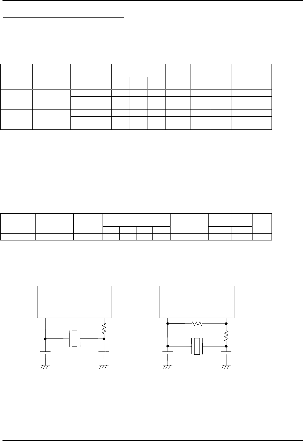
Figure 1 Ceramic oscillation circuit Figure 2 Crystal oscillation circuit
C3
Rd2
C4
X’tal
XT2 XT1
Rf
C1
C2
CF
CF2 CF1
Rd1
LC876694B/78B/62B
No.6843-21/23
Figure 3 AC timing measurement point
Reset time and oscillation stable time
HOLD release signal and oscillation stable time
Figure 4 Oscillation stablization time
0.5VDD
Power Suppl
y
RES
Internal RC
Resonator oscillation
CF1
,
CF2
XT1
,
XT2
Operation mode
Reset time
tmsCF
tmsXtal
Unfixed
Reset Instruction execution mode
VDD
VDD limit
0V
Internal RC
Resonator oscillation
CF1,CF2
XT1,XT2
Operation mode
HOLD release signal
Without HOLD
Release signal
HOLD release signal VALID
tmsCF
tmsXtal
HOLD HALT
PREVIOUS12345678NEXT