Closed Dec 25th-26th
800-300-1968
We Stock Hard to Find Parts
My Account
|
My Orders
|
My Cart
Questions?
(800) 300-1968
Register
(current)
My Account
(current)
My Orders
(current)
My Cart
(current)
Categories
(current)
Manufacturers
Request a Quote
Sell Your Excess
Consignment
Quality Assurance
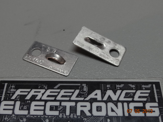
TC105
Part #
TC105
Description
CABLE TIE MTG BASE, ALUMINUM,25.4MM L X 12.7MM W, Mountin
Category
CLAMP
Availability
Out of Stock
Qty
0
Qty
Price
1 +
$0.29400
Related Items
ALL ELECTRONICS HARDWARE INC.
CLAMP
04-03-40-N
Military Spec
CORE
0444173551-0
$2.39799
ITT CANNON
CLAMP
057-3013-000
$60.44543
ITT CANNON
CLAMP
057-3013-013
$75.10311
Amphenol
CLAMP
10-101987-123
$10.52470
Generic
CLAMP
10-804941-202
$37.66404