WMS7140/1
Publication Release Date: April 21, 2005
- 17 - Revision 1.1
11.1.
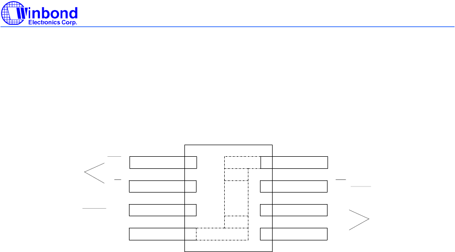
LAYOUT CONSIDERATIONS
Use a 0.1µF bypass capacitor as close as possible to the V
DD
pin. This is recommended for best
performance. Often this can be done by placing the surface mount capacitor on the bottom side of the
PC board, directly between the V
DD
and V
SS
pins. Care should be taken to separate the analog and
digital traces. Sensitive traces should not run under the device or close to the bypass capacitors.
A dedicated plane for analog ground helps in reducing ground noise for sensitive analog signals.
CAP
V
DD
CS
V
B
V
W
INC
U/D
V
A
V
SS
ANALOG
SIGNAL LINES
DIGITAL
CONTROL LINES
ANALOG
SIGNAL LINE
DIGITAL
CONTROL LINE
FIGURE 9 – WMS7140/1 LAYOUT


