Freelance Electronics Components Distributor
Closed Dec 25th-26th
800-300-1968
We Stock Hard to Find Parts

141050

Part # 141050
Description TYPE I 42VDC 50 AMPAUTO RESET PANEL MOUNT
Category CIRCUIT BREAKER
Availability Available With Additional Lead Time
Qty 199
Qty Price
1 - 99 $27.52750
100 - 999 $20.59904
1,000 - 4,999 $18.90504
5,000 - 9,999 $17.56678
10,000 + $11.61600
Manufacturer Available Qty
Optifuse
  • Factory Stock: Shipping 199
    Ships within 2-5 days
  • Additional Qty
      Lead Time:
    12 weeks


Technical Document


DISCLAIMER: The information provided herein is solely for informational purposes. Customers must be aware of the suitability of this product for their application, and consider that variable factors such as Manufacturer, Product Category, Date Codes, Pictures and Descriptions may differ from available inventory.

WMS7140/1
Publication Release Date: April 21, 2005
- 13 - Revision 1.1
PARAMETERS SYMBOL MIN. TYP. MAX. UNITS CONDITIONDS
Output Low Voltage V
OL
0.4 V I
OL
=2mA
Input Leakage Current I
LI
-1 +1 uA
CS =V
DD
,Vin=Vss ~ V
DD
Output Leakage Current
I
Lo
-1 +1 uA
CS =V
DD
,Vin=V
SS
~ V
DD
Input Capacitance
[1]
C
IN
25 pF V
DD
=5V, fc = 1Mhz
Output Capacitance
[1]
C
OUT
25 pF V
DD
=5V, fc = 1Mhz
Power Requirements
Operating Voltage V
DD
2.7 5.5 V
Operating Current I
DDR
0.5 1 mA
All ops except NVMEM
program
Operating Current I
DDW
1 2 mA
During Non-volatile
memory program
I
SA
[3]
0.5 1 mA
Buffer is active, NOP, no
load
Standby Current
I
SB
[4]
0.1 1 uA
Buffer is inactive, Power
Down, No load
Power Supply Rejection
Ratio
PSRR 1 LSB/V
V
DD
=5V±10%, Code=80H
Notes:
[1] Not subject to production test.
[2] LSB = (V
A
- V
B
) / (T- 1); DNL = (V
i+1
- V
i
) / LSB; INL = (V
i
- i*LSB) / LSB;
where i = [0, (T -1)] and T = # of taps of the device.
[3] WMS71x1 only.
[4] WMS71x0 only.
WMS7140/1
- 14 -
10.1
TEST CIRCUITS
FIGURE 4 – TEST CIRCUITS
Potentiometer divider nonlinearit
y
error
test circuit
INL, DNL
)
*Assume infinite in
p
ut im
p
edance
V+
V
MS
*
V+
= V
DD
1LSB= V+/256
WMS71xx
V
A
V
B
V
W
Resistor
p
osition nonlinearit
y
error test
circuit (Rheostat Operation: R-INL, R-DNL)
*Assume infinite in
p
ut im
p
edance
No Connection
V
MS
*
WMS71xx
W
V
A
V
B
V
W
I
W
WMS71xx
Wi
p
er resistance test circuit
*Assume infinite in
p
ut im
p
edance
V
MS
*
WMS71xx
V
A
V
B
V
W
I
W
I
W
= V
DD
/R
Total
R
W
= V
MS
/I
W
Power supply sensitivity test circuit (PSS, PSRR)
*Assume infinite in
p
ut im
p
edance
V
+
V
+
= V
DD
±
10%
V
A
V
B
V
W
V
MS
*
PSRR
(
dB
)
= 20LOG
(
)
V
MS
V
DD
PSS
(
%/%
)
=
V
MS
V
DD
WMS71xx
V
A
V
B
V
W
V
IN
~
+5V
2.5V DC
Offset
V
OUT
Ca
p
acitance test circuit
V
A
V
B
WMS71xx
V
W
V
IN
~
+5V
2.5V DC
V
OUT
OFFSET
GND
Gain
vs. fre
q
uenc
y
test circuit
WMS7140/1
Publication Release Date: April 21, 2005
- 15 - Revision 1.1
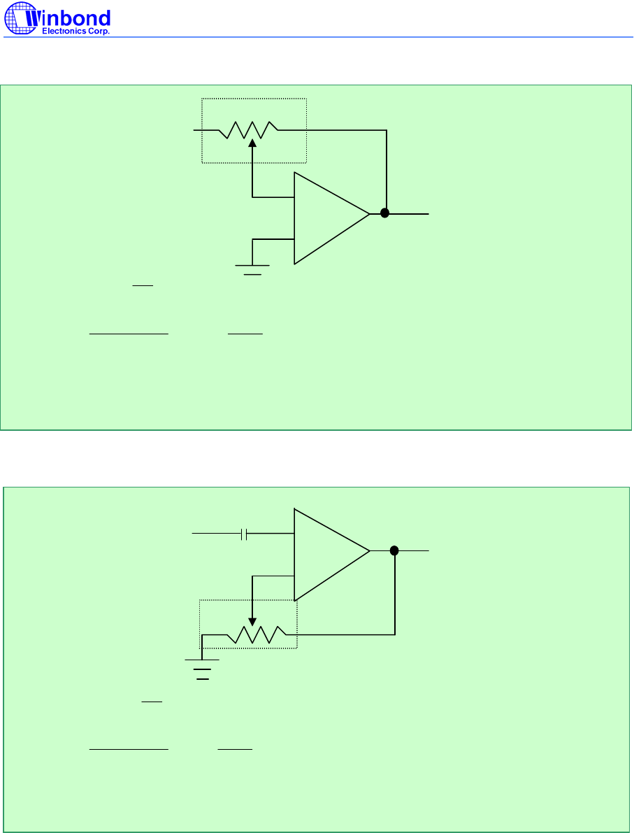
11. TYPICAL APPLICATION CIRCUITS
Vin
V
OUT
= - V
IN
A
B
R
R
R
A
=
256
D)(256R
AB
, R
B
=
256
DR
AB
R
AB
= Total resistance of potentiometer
D = Wiper setting for WMS71XX
FIGURE 5 – PROGRAMMABLE INVERTING GAIN AMPLIFIER USING THE WMS7140/1
V
OUT
= V
IN
(1+
A
B
R
R
)
R
A
=
256
D)(256R
AB
, R
B
=
256
DR
AB
R
AB
= Total resistance of potentiometer
D = Wiper setting for WMS71XX
FIGURE 6 – PROGRAMMABLE NON-INVERTING GAIN AMPLIFIER USING THE WMS7140/1
OP
A
MP
_
V
OUT
WMS71XX
+
OP
A
MP
V
IN
V
OUT
WMS71XX
_
R
A
R
B
R
A
R
B
+
PREVIOUS12345678NEXT