Closed Dec 25th-26th
800-300-1968
We Stock Hard to Find Parts
My Account
|
My Orders
|
My Cart
Questions?
(800) 300-1968
Register
(current)
My Account
(current)
My Orders
(current)
My Cart
(current)
Categories
(current)
Manufacturers
Request a Quote
Sell Your Excess
Consignment
Quality Assurance
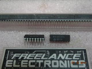
MC10125P
Part #
MC10125P
Description
Translator MECL to TTL 16-PinPDIP Rail
Category
IC
Availability
In Stock
Qty
4
Qty
Price
1 +
$2.39799
Manufacturer
Available
Qty
Motorola Corp
Date Code: 9600
Freelance Stock:
2
Ships Immediately
Motorola Corp
Date Code: 9143
Freelance Stock:
2
Ships Immediately
Add to Cart
Related Items
Motorola Corp
IC
MC10100L
$8.21872
Motorola Corp
IC
MC10101LD
$12.72913
Motorola Corp
IC
MC10102L
$1.79850
Motorola Corp
IC
MC10102LDS
$12.72913
Motorola Corp
IC
MC10102P
$3.07076
Motorola Corp
IC
MC10105L
$2.07618