Freelance Electronics Components Distributor
Closed Dec 25th-26th
800-300-1968
We Stock Hard to Find Parts

MAX186ACWP

Part # MAX186ACWP
Description IC DAS 8CH 12BIT T/H LP 20-SOIC
Category IC
Availability In Stock
Qty 72
Qty Price
1 - 15 $17.49752
16 - 30 $13.91849
31 - 45 $13.12314
46 - 60 $12.19524
61 + $10.86967
Manufacturer Available Qty
MAXIM
Date Code: 0627
  • Shipping Freelance Stock: 72
    Ships Immediately


Technical Document


DISCLAIMER: The information provided herein is solely for informational purposes. Customers must be aware of the suitability of this product for their application, and consider that variable factors such as Manufacturer, Product Category, Date Codes, Pictures and Descriptions may differ from available inventory.

MAX186/MAX188
;set delay between transfers
LDD #$0800
STD SPCR2 ;set ENDQP to $8 for 9 transfers
***** Initialize QSPI Command RAM *****
LDAA #$80 ;CONT=1,BITSE=0,DT=0,DSCK=0,PCS0=ACTIVE
STAA $FD40 ;store first byte in COMMAND RAM
LDAA #$C0 ;CONT=1,BITSE=1,DT=0,DSCK=0,PCS0=ACTIVE
STAA $FD41
STAA $FD42
STAA $FD43
STAA $FD44
STAA $FD45
STAA $FD46
STAA $FD47
LDAA #$40 ;CONT=0,BITSE=1,DT=0,DSCK=0,PCS0=ACTIVE
STAA $FD48
***** Initialize QSPI Transmit RAM *****
LDD #$008F
STD $FD20
LDD #$00CF
STD $FD22
LDD #$009F
STD $FD24
LDD #$00DF
STD $FD26
LDD #$00AF
STD $FD28
LDD #$00EF
STD $FD2A
LDD #$00BF
STD $FD2C
LDD #$00FF
STD $FD2E
LDD #$0000
STD $FD30
PULB
PULA
RTS
READ186:
;This routine triggers the QSPI microsequencer to autonomously
;trigger conversions on all 8 channels of the MAX186. Each
;conversion result is stored in the receive data RAM.
PSHA
LDAA #$80
ORAA SPCR1
STAA SPCR1 ;just set SPE
PULA
RTS
***** Interrupts/Exceptions *****
BDM: BGND ;exception vectors point here
Low-Power, 8-Channel,
Serial 12-Bit ADCs
22 ______________________________________________________________________________________
Figure 20. MAX186/MAX188 Assembly-Code Listing (continued)
MAX186/MAX188
Low-Power, 8-Channel,
Serial 12-Bit ADCs
______________________________________________________________________________________ 23
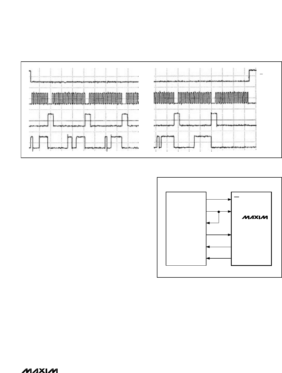
TMS320C3x to MAX186 Interface
Figure 22 shows an application circuit to interface the
MAX186/MAX188 to the TMS320 in external clock
mode. The timing diagram for this interface circuit is
shown in Figure 23.
Use the following steps to initiate a conversion in the
MAX186/MAX188 and to read the results:
1) The TMS320 should be configured with CLKX (trans-
mit clock) as an active-high output clock and CLKR
(TMS320 receive clock) as an active-high input clock.
CLKX and CLKR of the TMS320 are tied together with
the SCLK input of the MAX186/MAX188.
2) The MAX186/MAX188 CS is driven low by the XF_
I/O port of the TMS320 to enable data to be clocked
into DIN of the MAX186/MAX188.
3) An 8-bit word (1XXXXX11) should be written to the
MAX186/MAX188 to initiate a conversion and place
the device into external clock mode. Refer to Table
2 to select the proper XXXXX bit values for your spe-
cific application.
4) The SSTRB output of the MAX186/MAX188 is moni-
tored via the FSR input of the TMS320. A falling
edge on the SSTRB output indicates that the conver-
sion is in progress and data is ready to be received
from the MAX186/MAX188.
XF
CLKX
CLKR
DX
DR
FSR
CS
SCLK
DIN
DOUT
SSTRB
TMS320C3x
MAX186
MAX188
Figure 22. MAX186/MAX188 to TMS320 Serial Interface
• • • •
• • • •
• • • •
• • • •
CS
SCLK
SSTRB
DIN
Figure 21. QSPI Assembly-Code Timing
5) The TMS320 reads in one data bit on each of the
next 16 rising edges of SCLK. These data bits rep-
resent the 12-bit conversion result followed by four
trailing bits, which should be ignored.
6) Pull CS high to disable the MAX186/MAX188 until
the next conversion is initiated.
MAX186EVKIT-DIP Through-Hole
MAX188_MJP
Maxim cannot assume responsibility for use of any circuitry other than circuitry entirely embodied in a Maxim product. No circuit patent licenses are
implied. Maxim reserves the right to change the circuitry and specifications without notice at any time.
24
____________________________Maxim Integrated Products, 120 San Gabriel Drive, Sunnyvale, CA 94086 (408) 737-7600
© 1996 Maxim Integrated Products Printed USA is a registered trademark of Maxim Integrated Products.
MAX186/MAX188
Low-Power, 8-Channel,
Serial 12-Bit ADCs
PART
PIN-PACKAGE
MAX188_CPP 20 Plastic DIP
MAX188_CWP 20 SO
MAX188_CAP 20 SSOP
MAX188DC/D Dice*
MAX188_EPP Plastic DIP
-55°C to +125°C
TEMP. RANGE
0°C to +70°C
0°C to +70°C
0°C to +70°C
-40°C to +85°C
20 CERDIP**
MAX188_EWP 20 SO
MAX188_EAP -40°C to +85°C 20 SSOP
_Ordering Information (continued)
CS
SCLK
DIN
SSTRB
DOUT
START SEL2 SEL1 SEL0 UNI/BIP SGL/DIF PD1 PD0
MSB B10 B1 LSB
HIGH
IMPEDANCE
HIGH
IMPEDANCE
Figure 23. TMS320 Serial Interface Timing Diagram
___________________Chip Topography
V
DD
I/O
SCK (SK)*
MOSI (SO)
MISO (SI)
V
SS
SHDN
SSTRB
DOUT
DIN
SCLK
CS
V
SS
AGND
DGND
V
DD
REFADJ
CH7
C3
0.1µF
C4 
0.1µF
CH0
+5V
C2 
0.01µF
0V to
4.096V
ANALOG
INPUTS
MAX186
CPU
C1
4.7µF
VREF
__________Typical Operating Circuit
PART BOARD TYPETEMP. RANGE
0°C to +70°C
0°C to +70°C
-40°C to +85°C
NOTE: Parts are offered in grades A, B, C and D (grades defined
in Electrical Characteristics). When ordering, please specify grade.
* Dice are specified at +25°C, DC parameters only.
* * Contact factory for availability and processing to MIL-STD-883.
CH2
CH7
CH6
CH5
CH4
CH3
CH0CH1
V
DD
SCLK
CS
DIN
SSTRB
DOUT
DGND
AGND
AGNDV
SS
SHDN VREF REFADJ
0.151"
(3.84 mm)
0.117"
(2.97 mm)
MAX186/MAX188
TRANSISTOR COUNT: 2278;
SUBSTRATE CONNECTED TO V
DD
PREVIOUS12345678