Freelance Electronics Components Distributor
Closed Dec 25th-26th
800-300-1968
We Stock Hard to Find Parts

LT1014ACJ

Part # LT1014ACJ
Description OP Amp Quad GP ±22V/44V14-Pin CDip
Category IC
Availability In Stock
Qty 4
Qty Price
1 - 2 $52.06735
3 + $39.44496
Manufacturer Available Qty
Linear Technology
Date Code: 8842
  • Shipping Freelance Stock: 4
    Ships Immediately


Technical Document


DISCLAIMER: The information provided herein is solely for informational purposes. Customers must be aware of the suitability of this product for their application, and consider that variable factors such as Manufacturer, Product Category, Date Codes, Pictures and Descriptions may differ from available inventory.

7
LT1013/LT1014
TYPICAL PERFORMANCE CHARACTERISTICS
U
W
Voltage Gain vs Frequency
FREQUENCY (Hz)
0.01 0.1
VOLTAGE GAIN (dB)
1M 10M
110
100 1k
10k 100k
140
120
100
80
60
40
20
0
–20
V
S
= ±15VV
S
= 5V, 0V
T
A
= 25°C
C
L
= 100pF
LOAD RESISTANCE TO GROUND ()
100
100k
VOLTAGE GAIN (V/V)
1M
10M
1k 10k
V
O
= 20mV TO 3.5V
WITH V
S
= 5V, 0V
T
A
= 25°C, V
S
= ±15V
T
A
= –55°C, V
S
= ±15V
T
A
= 125°C, V
S
= ±15V
T
A
= –55°C, V
S
= 5V, 0V
T
A
= 25°C, V
S
= 5V, 0V
T
A
= 125°C, V
S
= 5V, 0V
V
O
= ±10V WITH V
S
= ±15V
Output Short Circuit Current
vs Time
TIME FROM OUTPUT SHORT TO GROUND (MINUTES)
0
SHORT CIRCUIT CURRENT (mA)
SINKING SOURCING
1 2
40
30
20
10
0
10
20
30
–40
3
–55°C
25°C
25°C
125°C
125°C
–55°C
V
S
= ±15V
Voltage Gain vs Load
Resistance
APPLICATIONS INFORMATION
WUU
U
Single Supply Operation
The LT1013/1014 are fully specified for single supply
operation, i.e., when the negative supply is 0V. Input
common-mode range includes ground; the output swings
within a few millivolts of ground. Single supply operation,
however, can create special difficulties, both at the input
and at the output. The LT1013/LT1014 have specific
circuitry which addresses these problems.
At the input, the driving signal can fall below 0V— inad-
vertently or on a transient basis. If the input is more than
a few hundred millivolts below ground, two distinct prob-
lems can occur on previous single supply designs, such as
the LM124, LM158, OP-20, OP-21, OP-220, OP-221, OP-
420:
a) When the input is more than a diode drop below ground,
unlimited current will flow from the substrate (V
termi-
nal) to the input. This can destroy the unit. On the LT1013/
1014, the 400 resistors, in series with the input (see
schematic diagram), protect the devices even when the
input is 5V below ground.
Gain, Phase vs Frequency
FREQUENCY (MHz)
0.1 0.3
VOLTAGE GAIN (dB)
20
10
0
–10
PHASE SHIFT (DEGREES)
80
100
120
140
160
180
200
13 10
T
A
= 25°C
V
CM
= 0V
C
L
= 100pF
PHASE
±15V
5V, 0V
±15V
5V, 0V
GAIN
Channel Separation vs
Frequency
FREQUENCY (Hz)
10
CHANNEL SEPARATION (dB)
160
140
120
100
80
60
100k
100
1k
10k
1M
LIMITED BY
THERMAL
INTERACTION
R
S
= 1k
R
S
= 100
V
S
= ±15V
T
A
= 25°C
V
IN
= 20Vp-p to 5kHz
R
L
= 2k
LIMITED BY
PIN TO PIN
CAPACITANCE
8
LT1013/LT1014
APPLICATIONS INFORMATION
WUU
U
(b) When the input is more than 400mV below ground (at
25°C), the input stage saturates (transistors Q3 and Q4)
and phase reversal occurs at the output. This can cause
lock-up in servo systems. Due to a unique phase reversal
protection circuitry (Q21, Q22, Q27, Q28), the LT1013/
1014’s outputs do not reverse, as illustrated below, even
when the inputs are at –1.5V.
There is one circumstance, however, under which the phase
reversal protection circuitry does not function: when the
other op amp on the LT1013, or one specific amplifier of the
other three on the LT1014, is driven hard into negative
saturation at the output.
Phase reversal protection does not work on amplifier:
A when D’s output is in negative saturation. B’s and C’s
outputs have no effect.
B when C’s output is in negative saturation. A’s and D’s
outputs have no effect.
C when B’s output is in negative saturation. A’s and D’s
outputs have no effect.
D when A’s output is negative saturation. B’s and C’s
outputs have no effect.
At the output, the aforementioned single supply designs
either cannot swing to within 600mV of ground (OP-20) or
cannot sink more than a few microamperes while swing-
ing to ground (LM124, LM158). The LT1013/1014’s
all-NPN output stage maintains its low output resistance
and high gain characteristics until the output is saturated.
In dual supply operations, the output stage is crossover
distortion-free.
Comparator Applications
The single supply operation of the LT1013/1014 lends
itself to its use as a precision comparator with TTL
compatible output:
In systems using both op amps and comparators, the
LT1013/1014 can perform multiple duties; for example,
on the LT1014, two of the devices can be used as op amps
and the other two as comparators.
4V
LT1013/LT1014
NO PHASE REVERSAL
2V
4V
0V
6Vp-p INPUT, –1.5V TO 4.5V
4V
LM324, LM358, OP-20
EXHIBIT OUTPUT PHASE
REVERSAL
V
S
= 5V, 0V 50µs/DIV
4
2
0
100
0
V
S
= 5V, 0V 50µs/DIV
2
0
0
100
INPUT (mV) OUTPUT (V)
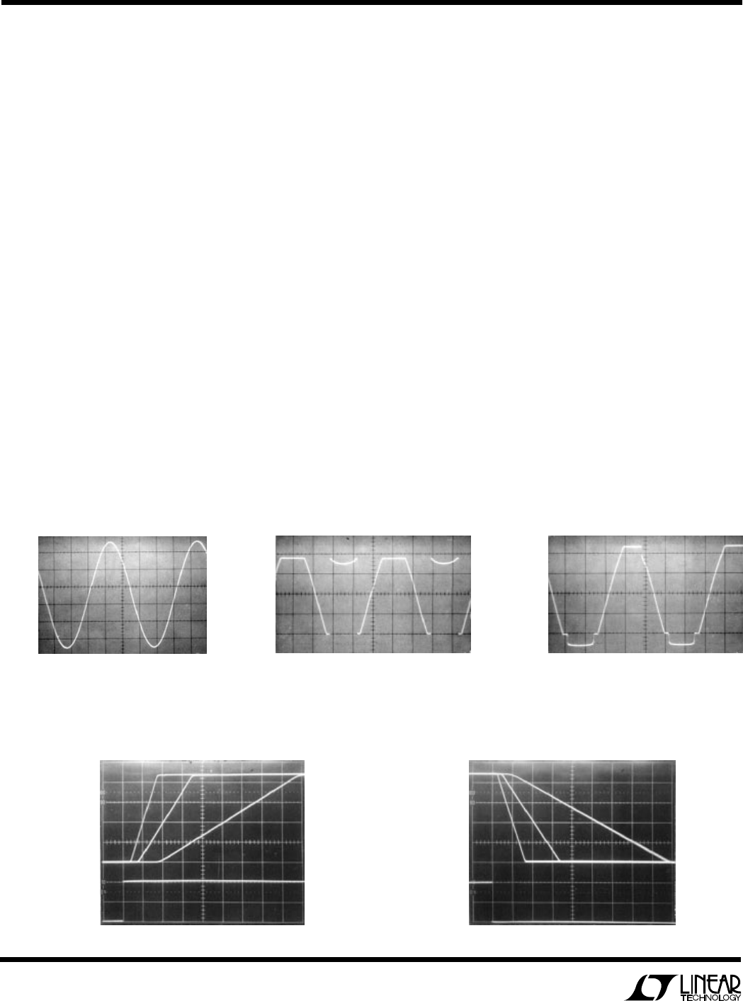
Voltage Follower with Input Exceeding the Negative Common-Mode Range
Comparator Rise Response Time
10mV, 5mV, 2mV Overdrives
Comparator Fall Response Time
to 10mV, 5mV, 2mV Overdrives
2V2V
0V0V
4
9
LT1013/LT1014
APPLICATIONS INFORMATION
WUU
U
Low Supply Operation
The minimum supply voltage for proper operation of the
LT1013/1014 is 3.4V (three Ni-Cad batteries). Typical
supply current at this voltage is 290µA, therefore power
dissipation is only one milliwatt per amplifier.
Noise Testing
For applications information on noise testing and calcula-
tions, please see the LT1007 or LT1008 data sheet.
Test Circuit for Offset Voltage and
Offset Drift with Temperature
+
LT1013
OR LT1014
+15V
15V
100*
50k*
50k*
V
O
RESISTOR MUST HAVE LOW
THERMOELECTRIC POTENTIAL.
THIS CIRCUIT IS ALSO USED AS THE BURN-IN 
CONFIGURATION, WITH SUPPLY VOLTAGES
INCREASED TO ±20V.
V
O
= 1000V
OS
*
**
TYPICAL APPLICATIONS
U
50MHz Thermal rms to DC Converter
+
+
LT1014
LT1014
8
10
9
7
4
11
6
5
0V–4V
OUTPUT
10k*
10k*10k*
10k*
10k
10k*
20k
FULL-
SCALE
TRIM
+5V
+
LT1014
14
13
12
10k*100k*
0.01
0.01
+
LT1014
1
2
3
100k*
0.01
300*
30k*
1µF
1µF
10k
10k
T1A T1B T2B T2A
BRN RED RED
GRN GRN
BRN
INPUT
300mV–
10V
RMS
+5V
2% ACCURACY, DC–50MHz.
100:1 CREST FACTOR CAPABILITY.
0.1% RESISTOR.
T1–T2 = YELLOW SPRINGS INST. CO. THERMISTOR COMPOSITE #44018.
ENCLOSE T1 AND T2 IN STYROFOAM.
7.5mW DISSIPATION.
*
30k*
+
1/2 LT1013
8
4
7
5
6
+5V
OUTPUT A
R2
R1
1µF
1µF
5
2
3
15
6
18
+INPUT
INPUT
+
1/2 LT1013
1
3
2
OUTPUT B
R2
R1
1µF
8
11
12
14
7
13
+INPUT
INPUT
1/2 LTC1043
1/2 LTC1043
16
0.01
OFFSET = 150µV
GAIN = + 1.
CMRR = 120dB.
COMMON-MODE RANGE IS 0V TO 5V.
R2
R1
1µF
5V Single Supply Dual Instrumentation Amplifier
PREVIOUS1234567NEXT